A surface-enhanced Raman substrate and its preparation method

A surface-enhanced Raman and substrate technology, applied in Raman scattering, nanotechnology for materials and surface science, material excitation analysis, etc., can solve problems such as high cost, unsuitable for large-scale industrial production, and cumbersome processes. Achieve controllable process, significant Raman enhancement effect, and simple manufacturing process

Active Publication Date: 2020-09-29
THE NAT CENT FOR NANOSCI & TECH NCNST OF CHINA
View PDF6 Cites 0 Cited by
  • Summary
  • Abstract
  • Description
  • Claims
  • Application Information

AI Technical Summary

Problems solved by technology

The whole process is not only cumbersome, but also costly, and is not suitable for large-scale industrial production

Method used


Image

  • A surface-enhanced Raman substrate and its preparation method
  • A surface-enhanced Raman substrate and its preparation method
  • A surface-enhanced Raman substrate and its preparation method

Examples


Embodiment 1

[0057] 1) Use magnetron sputtering to coat a layer of 200nm silver film on the silicon wafer to obtain a silver-coated silicon wafer;

[0058] 2) Put the silver-coated silicon wafer obtained in 1) into the ICP chamber of an inductively coupled plasma etching machine, and feed 30 sccm of working gas, wherein the working gas is composed of Cl with a volume ratio of 2:1. 2 and Ar, adjust the cavity pressure to 0.4Pa, set the power of the upper electrode to 500W, and set the power of the lower electrode to 60W, and maintain it for 30s to obtain a surface-enhanced Raman substrate.

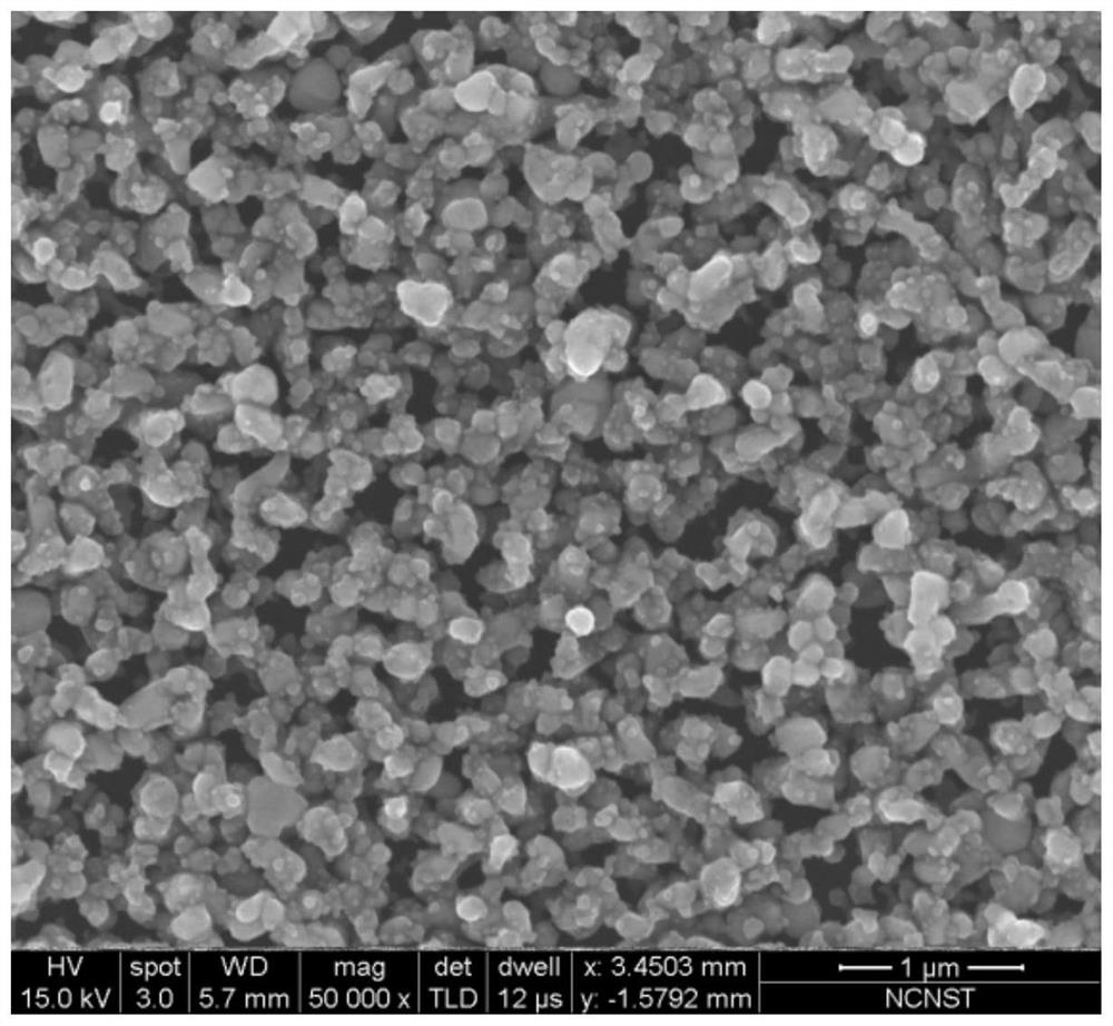
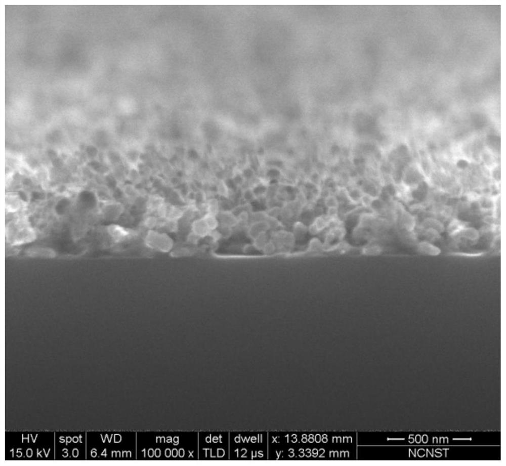
[0059] From figure 1 and figure 2 It can be seen that the surface of the surface-enhanced Raman substrate obtained in Example 1 forms a porous nano-silver film composed of nano-silver particles with a median diameter of about 30 nm uniformly dispersed on the surface of the silicon wafer.

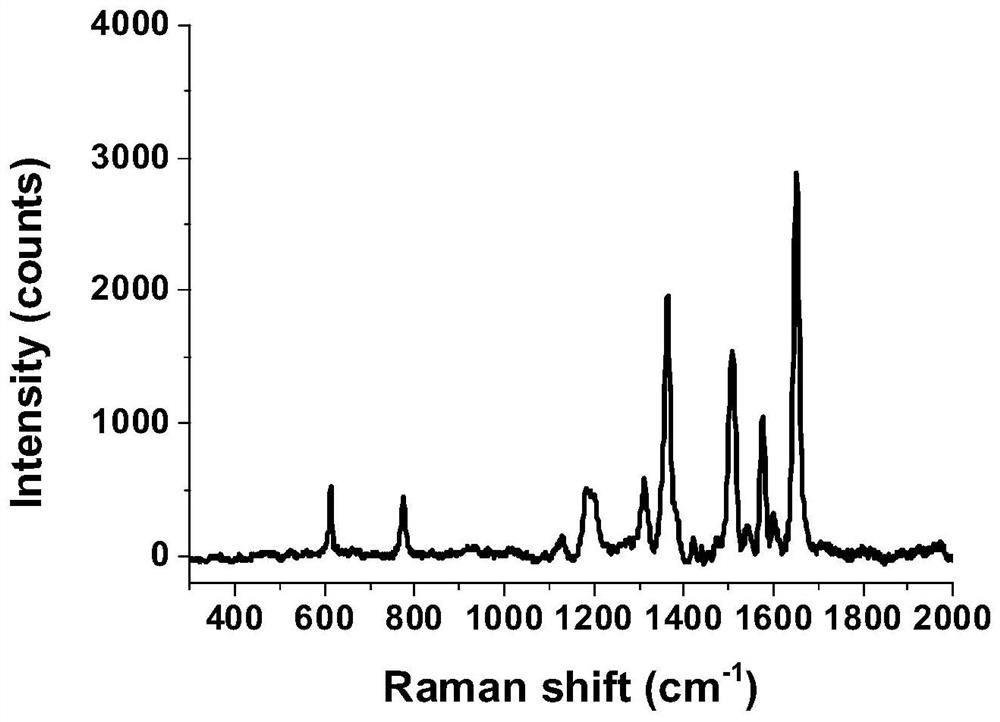
[0060] Take out the sample piece and modify the rhodamine 6G molecule: at 10 -7 Soak in mol / L rhodamine 6G solu...

Embodiment 2

[0064] 1) Use magnetron sputtering to plate a layer of 500nm silver film on the silicon wafer to obtain a silver-coated silicon wafer;

[0065] 2) Put 1) gained silver-coated film silicon chip into the ICP chamber of inductively coupled plasma etching machine, pass into the Cl of 50sccm 2 , the chamber pressure is 1Pa, the power of the upper electrode is set to 1000W, the power of the lower electrode is set to 100W, and it is maintained for 15s. The obtained surface-enhanced Raman substrate has high sensitivity and can realize single-molecule detection.

Embodiment 3

[0066] The difference between embodiment 3 and embodiment 2 is only that the etching time is 30s.

[0067] From Figure 4 and Figure 5 It can be seen that the surface of the surface-enhanced Raman substrate obtained in Example 3 forms a porous nano-silver film composed of nano-silver particles with a median diameter of about 40 nm uniformly dispersed on the surface of the silicon wafer. This surface-enhanced Raman substrate has high sensitivity and can realize single-molecule detection.


PUM

PropertyMeasurementUnit
thicknessaaaaaaaaaa
thicknessaaaaaaaaaa
poweraaaaaaaaaa

Abstract

The invention provides a preparation method of a surface-enhanced Raman substrate. The method comprises the following steps of preparing a silver film on a substrate to obtain a silver-plated substrate; and carrying out plasma dry etching on the silver-plated substrate to obtain the surface-enhanced Raman substrate with a porous structure. A silver porous structure with an adjustable particle size can be prepared, any mask is not needed, the preparation technology is simple, the process is controllable, the repeatability is good, and the surface-enhanced Raman substrate can be prepared in a large scale. The porous structure of prepared silver nanoparticles can be used as a surface-enhanced Raman efficient detection substrate; the Raman enhancement effect is significant; the detection substrate is good in performance consistency; and the sensitivity is high.

Description

technical field [0001] The invention relates to the technical field of micro-nano material processing, in particular to a surface-enhanced Raman substrate and a preparation method thereof. Background technique [0002] Surface-enhanced Raman scattering (SERS) detection technology has great practical application value in the fields of chemistry, biomedicine, and environmental detection. At the same time, SERS gives information at the molecular level, does not require ultra-high vacuum conditions, has high sensitivity and good selectivity, and uses non-destructive photons as probe signals, which has high sensitivity, simple detection process, low cost, and is easy to use in practice. implemented in the application. Up to 10 6 The enhancement effect has unique advantages compared to other surface detection technologies. Among many metals and noble metal materials, Ag usually shows the best enhancement effect. [0003] Due to its unique physical and chemical properties such ...

Claims


Application Information

Patent Timeline
Patent Type & Authority Patents(China)
IPC IPC(8): G01N21/65B82Y30/00B82Y40/00
CPCB82Y30/00B82Y40/00G01N21/658
Inventor 徐丽华褚卫国陈佩佩宋志伟田毅
Owner THE NAT CENT FOR NANOSCI & TECH NCNST OF CHINA
Why Eureka
Try Eureka