Preparation method for Ge-based heterogeneous solid-state plasma diode applied to annular antenna

A loop antenna and plasma technology, applied in the manufacture of semiconductor/solid-state devices, antennas, semiconductor devices, etc., can solve the problems of large injection dose and energy, low integration, high equipment requirements, etc., to suppress the impact, improve the breakdown voltage, good controllability

Active Publication Date: 2017-05-31
嘉兴奥腾电子科技有限公司
View PDF2 Cites 2 Cited by
  • Summary
  • Abstract
  • Description
  • Claims
  • Application Information

AI Technical Summary

Problems solved by technology

[0003] At present, there is a type of frequency reconfigurable antenna on the market. The material used in the solid-state plasma diode as an important component is bulk silicon material. This material has the problem of low carrier mobility in the intrinsic region, which affects the intrinsic region of the solid-state plasma diode. Carrier concentration, which in turn affects its solid-state plasma concentration; and the P region and N region of this structure are mostly formed by implantation process. This method requires a large implant dose and energy, requires high equipment, and is not compatible with existing processes. ; while the diffusion process is used, although the junction depth is deeper, but at the same time, the area of ​​the P region and the N region is relatively large, the degree of integration is low, and the doping concentration is uneven, which affects the electrical performance of the solid-state plasma diode, resulting in the concentration and distribution of the solid-state plasma. poor controllability

Method used


Image

  • Preparation method for Ge-based heterogeneous solid-state plasma diode applied to annular antenna
  • Preparation method for Ge-based heterogeneous solid-state plasma diode applied to annular antenna
  • Preparation method for Ge-based heterogeneous solid-state plasma diode applied to annular antenna

Examples


Embodiment 1

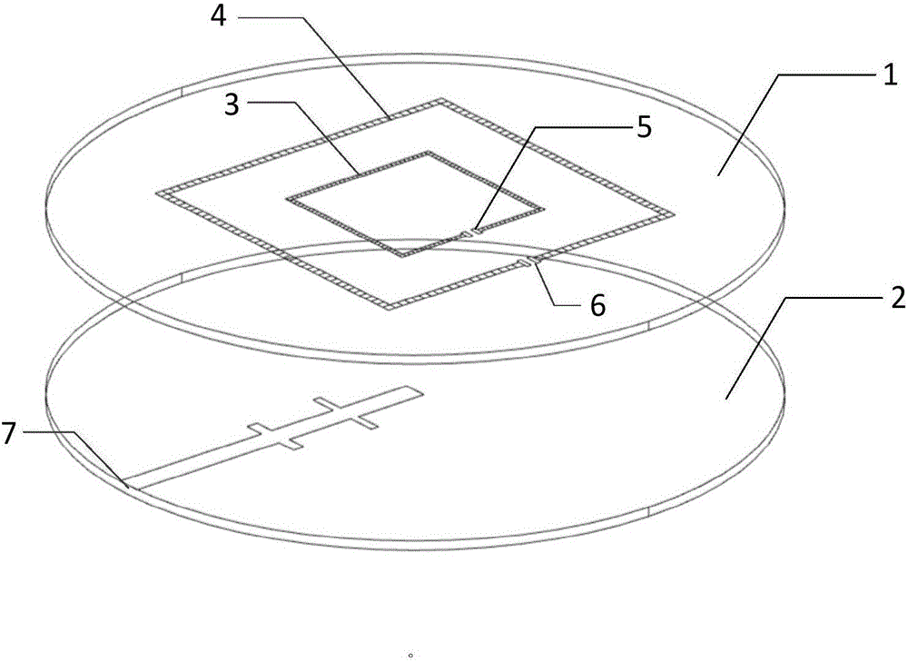
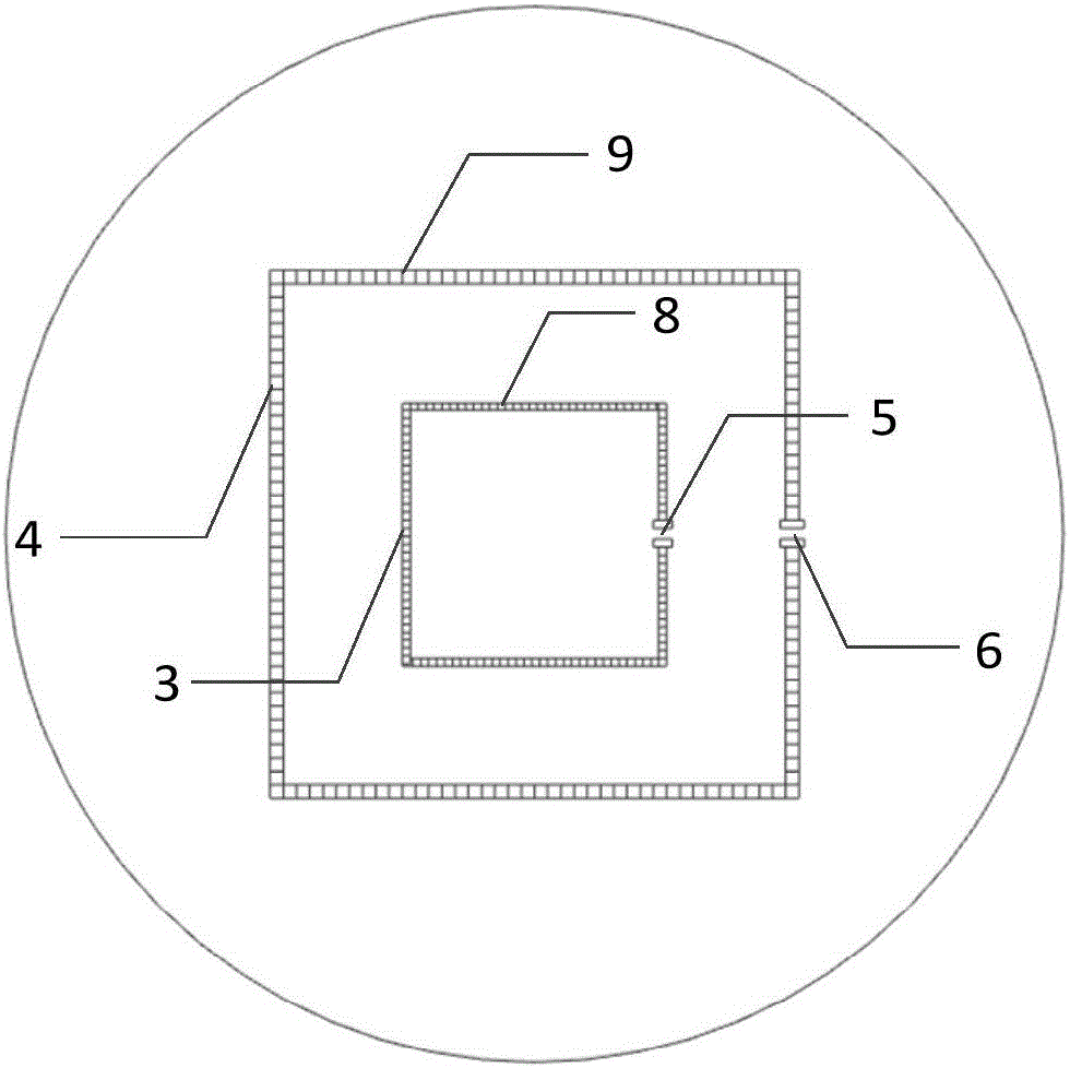
[0062] An embodiment of the present invention provides a method for preparing a Ge-based heterogeneous solid-state plasma diode applied to a loop antenna, and the Ge-based heterogeneous solid-state plasma diode is used to manufacture a reconfigurable loop antenna. Please refer to figure 1 , figure 1 It is a structural schematic diagram of a reconfigurable loop antenna according to an embodiment of the present invention; the loop antenna includes: a semiconductor substrate (1); a dielectric plate (2); a first solid-state plasma diode ring (3), a second solid-state plasma The diode ring (4), the first DC bias line (5) and the second DC bias line (6) are all arranged on the semiconductor substrate (1); the coupled feed source (7) is arranged on On the medium plate (2);

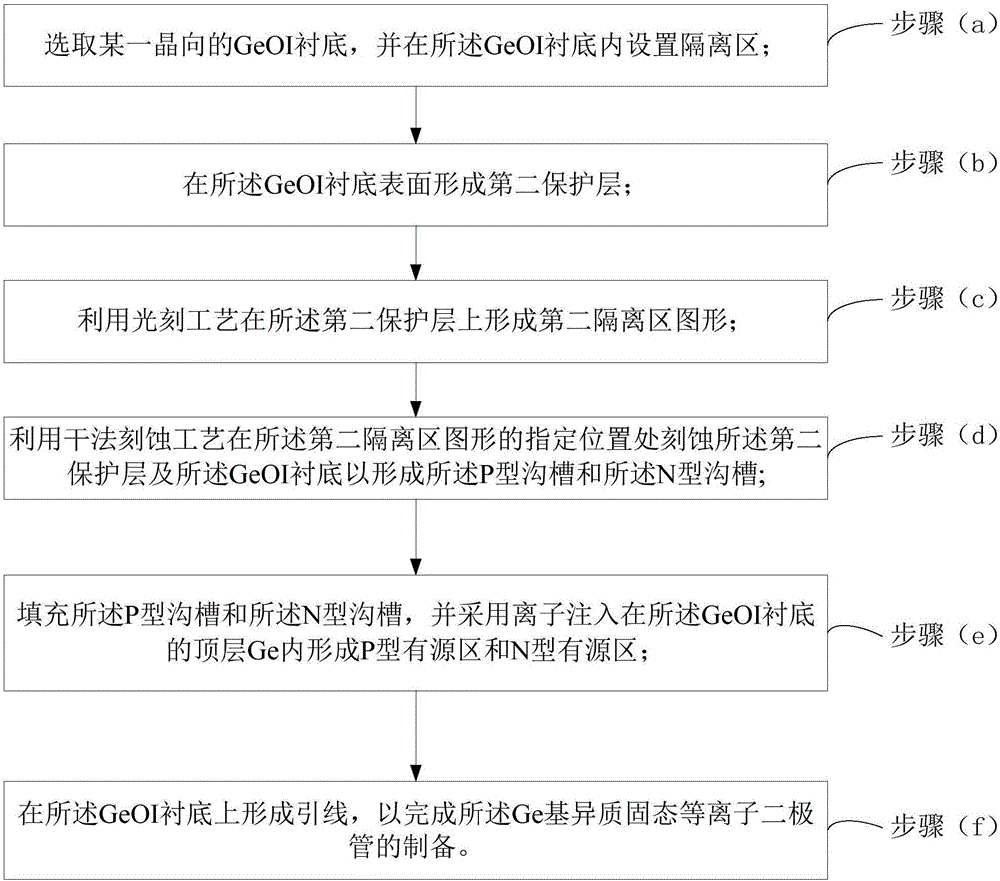
[0063] Please refer to figure 2 , figure 2 It is a flowchart of a method for preparing a Ge-based heterogeneous solid-state plasma diode according to an embodiment of the present invention. The preparation...

Embodiment 2

[0105] See Figure 7a-Figure 7r , Figure 7a-Figure 7r It is a schematic diagram of a method for preparing a Ge-based heterogeneous solid-state plasma diode according to an embodiment of the present invention. On the basis of the above-mentioned embodiment 1, to prepare a GeOI-based solid-state solid-state diode with a channel length of 22 nm (the length of the solid-state plasma region is 100 microns) The plasma diode is taken as an example for detailed description, and the specific steps are as follows:

[0106] Step 1, substrate material preparation steps:

[0107] (1a) if Figure 7a As shown, the (100) crystal orientation is selected, the doping type is p-type, and the doping concentration is 10 14 cm -3 A GeOI substrate sheet 101, the thickness of the top layer Ge is 50 μm;

[0108] (1b) if Figure 7b As shown, a first layer of SiO with a thickness of 40nm is deposited on a GeOI substrate by chemical vapor deposition (Chemical vapor deposition, CVD for short). 2 la...

Embodiment 3

[0135] Please refer to Figure 8 , Figure 8It is a schematic diagram of a device structure of a Ge-based heterogeneous solid-state plasma diode according to an embodiment of the present invention. The Ge-based heterogeneous solid-state plasmonic diode adopts the above-mentioned figure 1 The preparation method shown is made, specifically, the Ge-based solid-state plasma diode is prepared and formed on the GeOI substrate 301, and the P region 304, the N region 305 of the solid-state plasma diode and the laterally located P region 304 and the N region 305 The I regions in between are located in the top layer Ge302 of the GeOI substrate. Wherein, the solid-state plasma diode can be isolated by STI deep trenches, that is, an isolation trench 303 is provided outside the P region 304 and the N region 305, and the depth of the isolation trench 303 is greater than or equal to the thickness of the top layer Ge302.


PUM


Abstract

The invention relates to a preparation method for a Ge-based heterogeneous solid-state plasma diode applied to an annular antenna. The preparation method comprises the steps of selecting a GeOI substrate of a certain crystal orientation, and setting an isolation region on the GeOI substrate; forming a second protection layer on the surface of the GeOI substrate; forming a second isolation region pattern on the second protection layer through a photoetching process; etching the second protection layer and the GeOI substrate in appointed positions of the second isolation region pattern through a dry etching process to form a P type trench and an N type trench; filling the P type trench and the N type trench, and forming a P type active region and an N type active region in top layer Ge of the GeOI substrate by adopting ion implantation; and forming leads on the GeOI substrate to complete the preparation of the Ge-based heterogeneous solid-state plasma diode. According to the embodiments, the high-performance heterogeneous Ge-based solid-state plasma diode, which is applicable to formation of the solid-state plasma antenna, can be prepared through a deep trench isolation technology and an ion implantation process.

Description

technical field [0001] The invention relates to the technical field of semiconductor device manufacturing, in particular to a method for preparing a Ge-based heterogeneous solid-state plasma diode applied to a loop antenna. Background technique [0002] Nowadays, one of the important directions for the development of various communication systems is large capacity, multi-function, and ultra-wideband. By increasing system capacity, increasing system functions, and expanding system bandwidth. By increasing system capacity, increasing system functions, and controlling system bandwidth, on the one hand, the increasing actual demand can be met, and on the other hand, the system cost can also be reduced. As the front end of various wireless communication systems, the performance of the antenna has an important impact on the overall function of the communication system. Therefore, corresponding requirements such as multi-frequency, broadband, and miniaturization have been put forw...

Claims


Application Information

Patent Timeline
Patent Type & Authority Applications(China)
IPC IPC(8): H01L21/329H01Q23/00
CPCH01L29/6609H01Q23/00
Inventor 尹晓雪张亮
Owner 嘉兴奥腾电子科技有限公司
Why Eureka
Try Eureka