Power semiconductor device and preparation method thereof

A technology of power semiconductors and devices, which is applied in the field of power semiconductor devices and their preparation, and can solve problems such as increasing the difficulty of process control, the preparation process of power semiconductor devices needs to be improved, and large parameter fluctuations.

Inactive Publication Date: 2017-05-31
BYD CO LTD
View PDF4 Cites 5 Cited by
  • Summary
  • Abstract
  • Description
  • Claims
  • Application Information

AI Technical Summary

Problems solved by technology

In such a preparation process, the alignment deviation problem of P+ lithography and N+ lithography will cause fluctuations and deviations of device parameters (such as Vth)
Especially when the design margin is low, the parameters fluctuate greatly, which will increase the difficulty of process control and cause a high lithography rework rate, and reduce the product yield
[0004] Therefore, the preparation process of current power semiconductor devices still needs to be improved.

Method used


Image

  • Power semiconductor device and preparation method thereof
  • Power semiconductor device and preparation method thereof
  • Power semiconductor device and preparation method thereof

Examples


Embodiment Construction

[0026] Embodiments of the present invention are described in detail below. The embodiments described below are exemplary only for explaining the present invention and should not be construed as limiting the present invention. If no specific technique or condition is indicated in the examples, it shall be carried out according to the technique or condition described in the literature in this field or according to the product specification. The reagents or instruments used were not indicated by the manufacturer, and they were all commercially available conventional products.

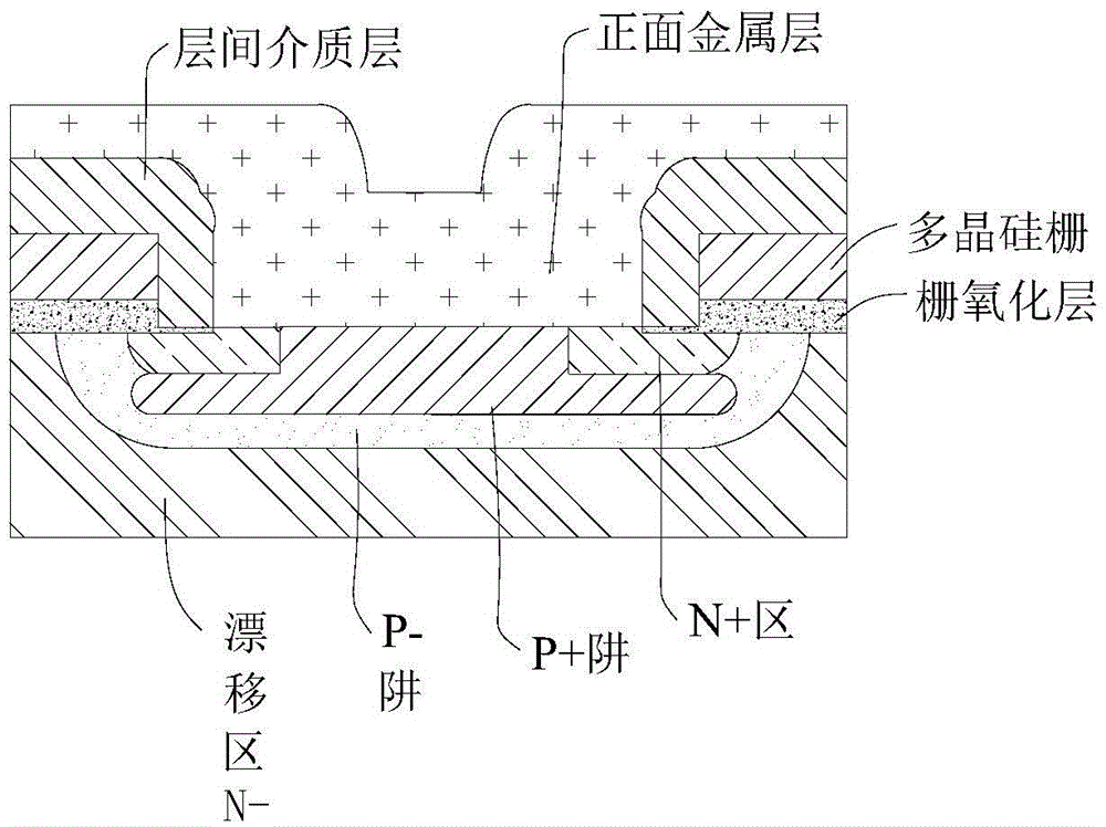
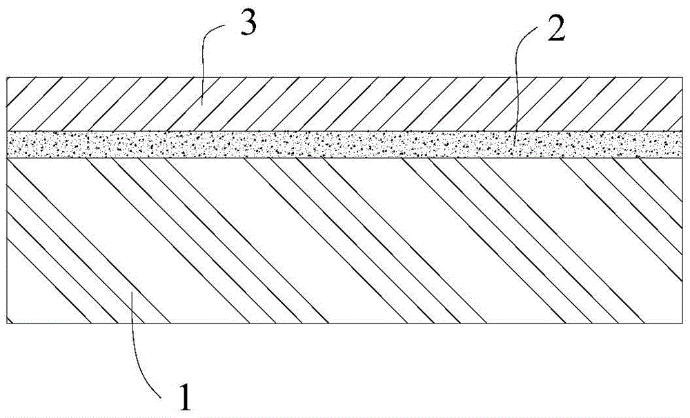
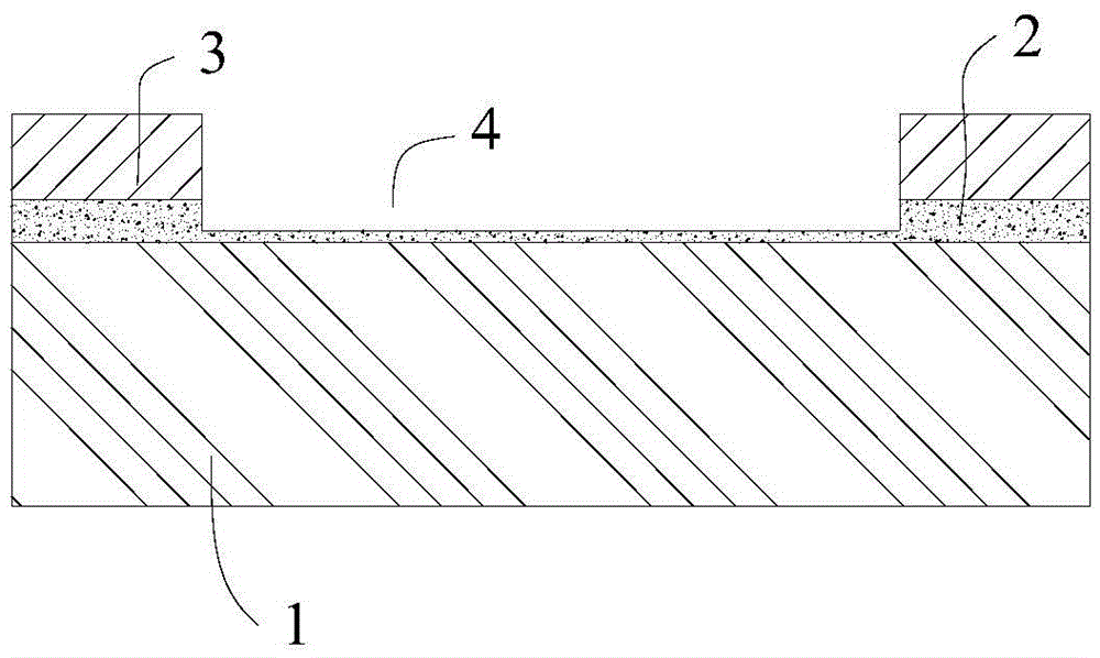
[0027] In one aspect of the invention, the invention provides a method of making a power semiconductor device. According to an embodiment of the present invention, refer to Figure 2A-Figure 2O , the method includes the following steps:

[0028] (1) Refer to Figure 2A , forming a gate oxide layer 2 on the upper surface of the substrate 1 , and depositing a polysilicon gate 3 on the upper surface of th...


PUM

PropertyMeasurementUnit
thicknessaaaaaaaaaa
heightaaaaaaaaaa

Abstract

The invention provides a power semiconductor device and a preparation method thereof. The method comprises the steps of forming a gate oxidation layer, and depositing a polycrystalline silicon gate; performing first etching treatment; performing first ion injection treatment; performing second ion injection treatment; forming a thermal oxidation layer; performing third ion injection treatment; depositing an interlayer dielectric layer; performing second etching treatment; and sputtering front-surface metal. According to the preparation method of the power semiconductor device, provided by an embodiment of the invention, general photoetching selective injection is replaced with a thermal oxidation layer self-alignment process and contact etching, so that the process steps can be effectively reduced, the process control difficulty can be lowered, the P+ and N+ photoetching rework rates and the parameter fluctuation and deviation caused by the P+ photoetching alignment and N+ photoetching alignment problems are avoided, the device parameter stability is improved, and the product yield is increased.

Description

technical field [0001] The invention relates to the technical field of semiconductors, in particular to a power semiconductor device and a preparation method thereof. Background technique [0002] Insulated gate bipolar transistor (Insulated Gate Bipolar Transistor, IGBT), vertical double diffused metal-oxide semiconductor field effect transistor (VDMOS) is a commonly used power semiconductor device (also known as power electronic device), which has the ability to handle high voltage, High current capability has been widely used in frequency conversion, voltage conversion, current conversion, power management and so on. [0003] Existing IGBT, VDMOS (structural schematic diagram see figure 1 ) preparation process generally includes: P-implantation, P+ photolithography, P+ implantation, P+ glue removal, P- / P+ well annealing, gate oxide etching, N+ photolithography, N+ implantation, N+ glue removal, making interlayer dielectric layer , contact hole photolithography, etching,...

Claims


Application Information

Patent Timeline
Patent Type & Authority Applications(China)
IPC IPC(8): H01L21/331H01L21/265H01L29/06H01L29/739
CPCH01L29/66325H01L21/26513H01L29/0684H01L29/7393
Inventor 郑忠庆
Owner BYD CO LTD
Why Eureka
Try Eureka