Material structure of GaN-base enhancement-mode electronic device

A material structure and electronic device technology, applied in the manufacture of electrical components, semiconductor devices, semiconductor/solid-state devices, etc., can solve the problems of fluorine ion implantation technology process repeatability, restricting technology industrialization, and difficulty, and achieve improved controllability Accuracy and consistency, solve the process repeatability, reduce the effect of on-resistance

Inactive Publication Date: 2017-05-31
INST OF MICROELECTRONICS CHINESE ACAD OF SCI
View PDF4 Cites 7 Cited by
  • Summary
  • Abstract
  • Description
  • Claims
  • Application Information

AI Technical Summary

Problems solved by technology

[0004] Groove etching is achieved by plasma dry etching of the Al(In, Ga)N barrier layer. Since the barrier layer is generally only about 20nm, it is difficult to achieve the same batch of different wafers through this technology, especially The repeatability of etching depth between different batches of wafers restricts the industrialization of this technology
Fluorine ion implantation technology also faces the problem of process repeatability

Method used


Image

  • Material structure of GaN-base enhancement-mode electronic device
  • Material structure of GaN-base enhancement-mode electronic device
  • Material structure of GaN-base enhancement-mode electronic device

Examples


Embodiment Construction

[0030] In order to make the object, technical solution and advantages of the present invention clearer, the present invention will be further described in detail below in conjunction with specific embodiments and with reference to the accompanying drawings.

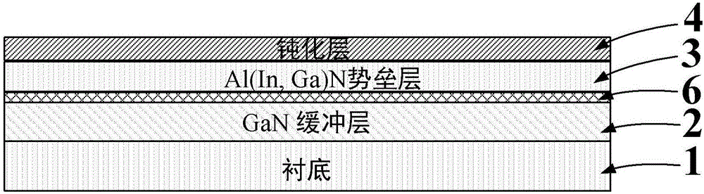
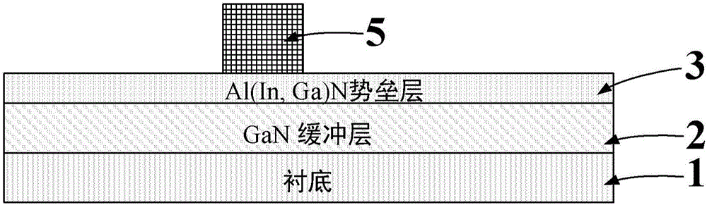
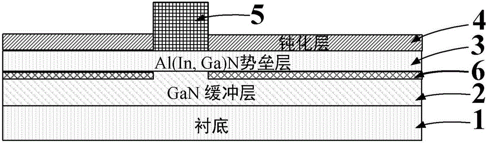
[0031] The material structure of the GaN-based enhanced electronic device provided by the present invention, such as figure 1 As shown, including: substrate; thin barrier Al(In, Ga)N / GaN heterostructure formed on the substrate; n-GaN formed on the thin barrier Al(In, Ga)N layer , SiO 2 or SiN x passivation layer.

[0032] figure 1 Among them, the thin barrier Al(In, Ga)N / GaN heterostructure is directly epitaxial GaN buffer layer and Al(In, Ga)N barrier layer on the substrate by metal-organic chemical vapor deposition or molecular beam epitaxy technology. And formed to realize the enhanced gate structure. In the thin barrier Al(In, Ga)N / GaN heterostructure, the Al(In, Ga)N barrier layer is an AlGaN or AlInN ternary al...


PUM

PropertyMeasurementUnit
thicknessaaaaaaaaaa
thicknessaaaaaaaaaa

Abstract

The invention discloses a material structure of a GaN-base enhancement-mode electronic device, and relates to the technical field of application of GaN-base power electronics and microwave power amplifiers. The material structure comprises a substrate, a GaN buffer layer and an Al(In,Ga)N barrier layer which are sequentially formed on the substrate, and a passivation layer, wherein the Al(In,Ga)N barrier layer forms a thin barrier Al(In,Ga)N/GaN heterostructure; and the passivation layer is formed on the thin barrier Al(In,Ga)N layer, and prepared from n-GaN, SiO2 or SiNx. Therefore, an enhancement-mode gate structure can be formed without etching the Al(In,Ga)N barrier layer; the density of two-dimensional electron gas in a thin barrier Al(In,Ga)N/GaN heterojunction channel outside a gate is significantly improved by utilizing polarization of the passivation layer or an n-type doping effect; the GaN-base enhancement-mode power electronic device with good threshold uniformity and low dynamic on resistance can be prepared; a yield of the device is increased; and an industrialization progress of the GaN-base power electronic device is pushed.

Description

technical field [0001] The invention relates to the technical field of GaN-based power electronics and microwave power amplifier applications, in particular to a material structure of a GaN-based enhanced electronic device. Background technique [0002] High-efficiency power electronic devices (also known as power switching devices) have great application value in the fields of smart grid, industrial control, new energy power generation, electric vehicles, and consumer electronics. More than 70% of the world's power electronic systems are powered by power semiconductor devices. Management system to control and manage. The performance of traditional Si power electronic devices is close to the physical limit of Si semiconductor materials. New wide-bandgap semiconductor devices represented by SiC and GaN are expected to become A strong contender for the next generation of high-efficiency power electronics. [0003] The enhanced type is a key requirement for the safe operation...

Claims


Application Information

Patent Timeline
Patent Type & Authority Applications(China)
IPC IPC(8): H01L29/06H01L29/778H01L21/335
CPCH01L29/7787H01L29/0638H01L29/0684H01L29/0688H01L29/66462
Inventor 黄森刘新宇王鑫华康玄武魏珂
Owner INST OF MICROELECTRONICS CHINESE ACAD OF SCI
Why Eureka
Try Eureka