Diamond substrate-based gallium nitride high-electron-mobility transistor and preparation method thereof

A high electron mobility, gallium nitride-based wafer technology, applied in semiconductor/solid-state device manufacturing, circuits, electrical components, etc., can solve the problems of difficult growth, poor material quality, large dislocation density, etc. Wrinkled or broken, good uniformity

Inactive Publication Date: 2017-05-31
NO 55 INST CHINA ELECTRONIC SCI & TECHNOLOGYGROUP CO LTD
View PDF7 Cites 28 Cited by
  • Summary
  • Abstract
  • Description
  • Claims
  • Application Information

AI Technical Summary

Problems solved by technology

However, the current method of directly epitaxially growing GaN on a diamond substrate has a lot of problems. Poor material quality, which prevents the performance advantages of GaN high electron mobility transistors based on diamond su

Method used


Image

  • Diamond substrate-based gallium nitride high-electron-mobility transistor and preparation method thereof
  • Diamond substrate-based gallium nitride high-electron-mobility transistor and preparation method thereof
  • Diamond substrate-based gallium nitride high-electron-mobility transistor and preparation method thereof

Examples


preparation example Construction

[0027] The present invention is based on a diamond substrate gallium nitride high electron mobility transistor and a preparation method thereof, comprising the following steps:

[0028] 1) Clean the silicon carbide-based gallium nitride wafer and the surface of the temporary slide with hydrochloric acid, rinse with deionized water, and then put it into a dryer for drying.

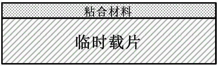
[0029] 2) Coating an adhesive material as a bonding material on the front side of the temporary carrier. The coating in the step 2) adopts the spin coating method, the rotating speed is 1000 rpm-3000 rpm, and the time is 30-60 seconds.

[0030] 3) Place the temporary slides face up on a hot plate and bake. The baking time in the step 3) is 2-5 minutes, and the temperature of the hot plate is 100-110 degrees Celsius.

[0031] 4) After the temporary carrier is naturally cooled at room temperature, the silicon carbide-based gallium nitride wafer and the temporary carrier are bonded facing each other. The bo...

Embodiment

[0039] The preparation method of the gallium nitride high electron mobility transistor based on the diamond substrate of the present invention is prepared by the following steps:

[0040] ①Preparation of samples: Soak GaN-on-SiC wafers and glass slides in dilute hydrochloric acid for 60 seconds, rinse with deionized water, blow dry with nitrogen, and finally dry the water thoroughly in an oven. Make sure the surface is clean and dry. Such as figure 1 , figure 2 shown.

[0041] ②Apply adhesive material on the front of the temporary slide: drop an appropriate amount of adhesive material on the front of the temporary slide, and spin coat at a rate of 1000-3000 rpm according to different thicknesses, and the spin coating time should not be less than 30 seconds After 10 minutes, place the temporary carrier coated with the adhesive material face up on the hot plate for pre-baking. The temperature of the hot plate is about 100-110 degrees Celsius, and the time is 2-5 minutes. If...


PUM


Abstract

The invention discloses a diamond substrate-based gallium nitride high-electron-mobility transistor and a preparation method thereof. The method comprises the following steps of firstly cleaning a silicon carbide-based gallium nitride wafer and the surface of a temporary slide; coating the front surface of the temporary slide with an adhesive material as a bonding material and putting the adhesive material on a hot plate for baking; oppositely bonding the silicon carbide-based gallium nitride wafer and the front surface of the temporary slide; carrying out thinning polishing and etching on a silicon carbide substrate of the silicon carbide-based gallium nitride wafer to remove the residual silicon carbide substrate; cleaning the surface of a gallium nitride epitaxial layer employing the temporary slide as a support; growing a layer of dielectric on the outer surface of the gallium nitride epitaxial layer employing the temporary slide as the support; carrying out epitaxial growth of a polycrystalline diamond substrate on the gallium nitride epitaxial layer employing the temporary slide as the support and automatically separating a diamond-based gallium nitride wafer from the temporary slide; and preparing the high-electron-mobility transistor on the diamond-based gallium nitride wafer. The limitation that original epitaxial growth is very difficult is broken, and epitaxial growth of diamond on gallium nitride can be relatively well controlled.

Description

technical field [0001] The invention belongs to the technical field of semiconductor technology, in particular to a gallium nitride high electron mobility transistor based on a diamond substrate and a preparation method thereof. Background technique [0002] Gallium nitride high electron mobility transistors, as the third-generation wide bandgap compound semiconductor devices, have the characteristics of high two-dimensional electron gas concentration, high breakdown field strength, and high electron saturation velocity. However, the power performance advantages of GaN high electron mobility transistors are far from being fully utilized. One of the main reasons is that GaN microwave power devices generate a lot of heat while outputting high power, but they cannot quickly and effectively dissipate the heat. Let it out. At present, gallium nitride materials are mainly epitaxially grown on silicon carbide, sapphire and other substrate materials (200610011228.6, 200810226288.9,...

Claims


Application Information

Patent Timeline
IPC IPC(8): H01L29/778H01L21/335H01L29/40
CPCH01L29/7783H01L29/402H01L29/66462
Inventor 吴立枢孔月婵
Owner NO 55 INST CHINA ELECTRONIC SCI & TECHNOLOGYGROUP CO LTD
Why Eureka
Try Eureka