Single row carrier photodetector and method of making the same

A photodetector, single-row carrier technology, applied in circuits, electrical components, semiconductor devices, etc., can solve problems such as difficulty in high-speed response, reduce space charge effects, achieve lattice matching, and improve saturation output current. Effect

Active Publication Date: 2018-10-30
SUZHOU SUNA PHOTOELECTRIC
View PDF4 Cites 0 Cited by
  • Summary
  • Abstract
  • Description
  • Claims
  • Application Information

AI Technical Summary

Problems solved by technology

For traditional PIN photodetectors, it is difficult to maintain high-speed response under high current density conditions due to the limitation of space charge effects

Method used


Image

  • Single row carrier photodetector and method of making the same
  • Single row carrier photodetector and method of making the same

Examples


Embodiment Construction

[0031] The technical solutions in the embodiments of the present invention will be described in detail below in conjunction with the accompanying drawings in the embodiments of the present invention. Obviously, the described embodiments are only some of the embodiments of the present invention, not all of them. Based on the embodiments of the present invention, all other embodiments obtained by persons of ordinary skill in the art without making creative efforts belong to the protection scope of the present invention.

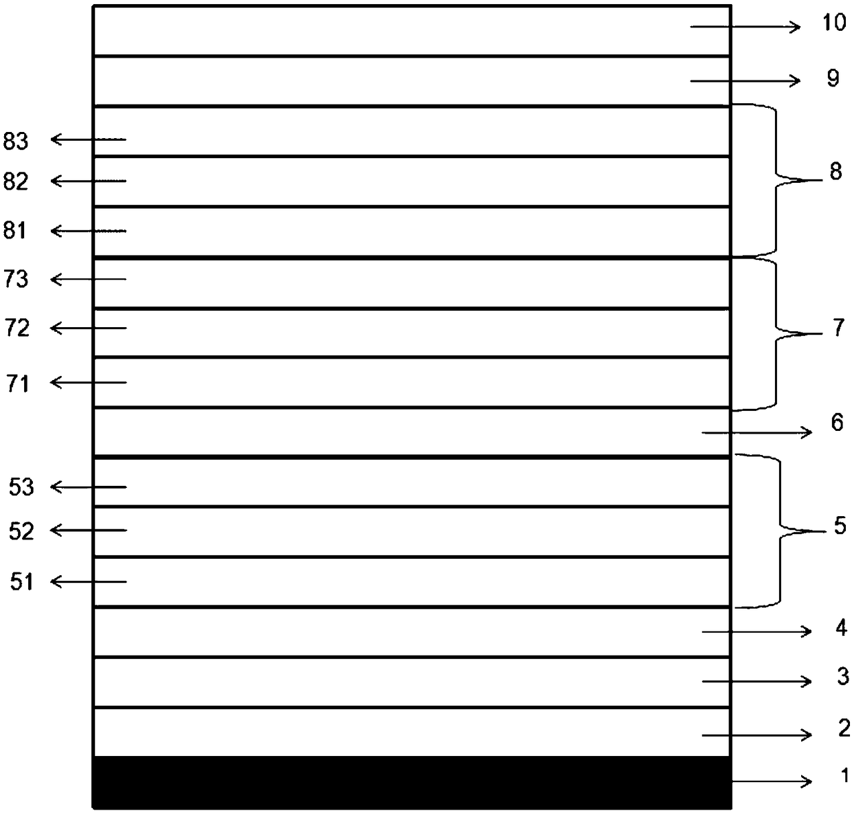
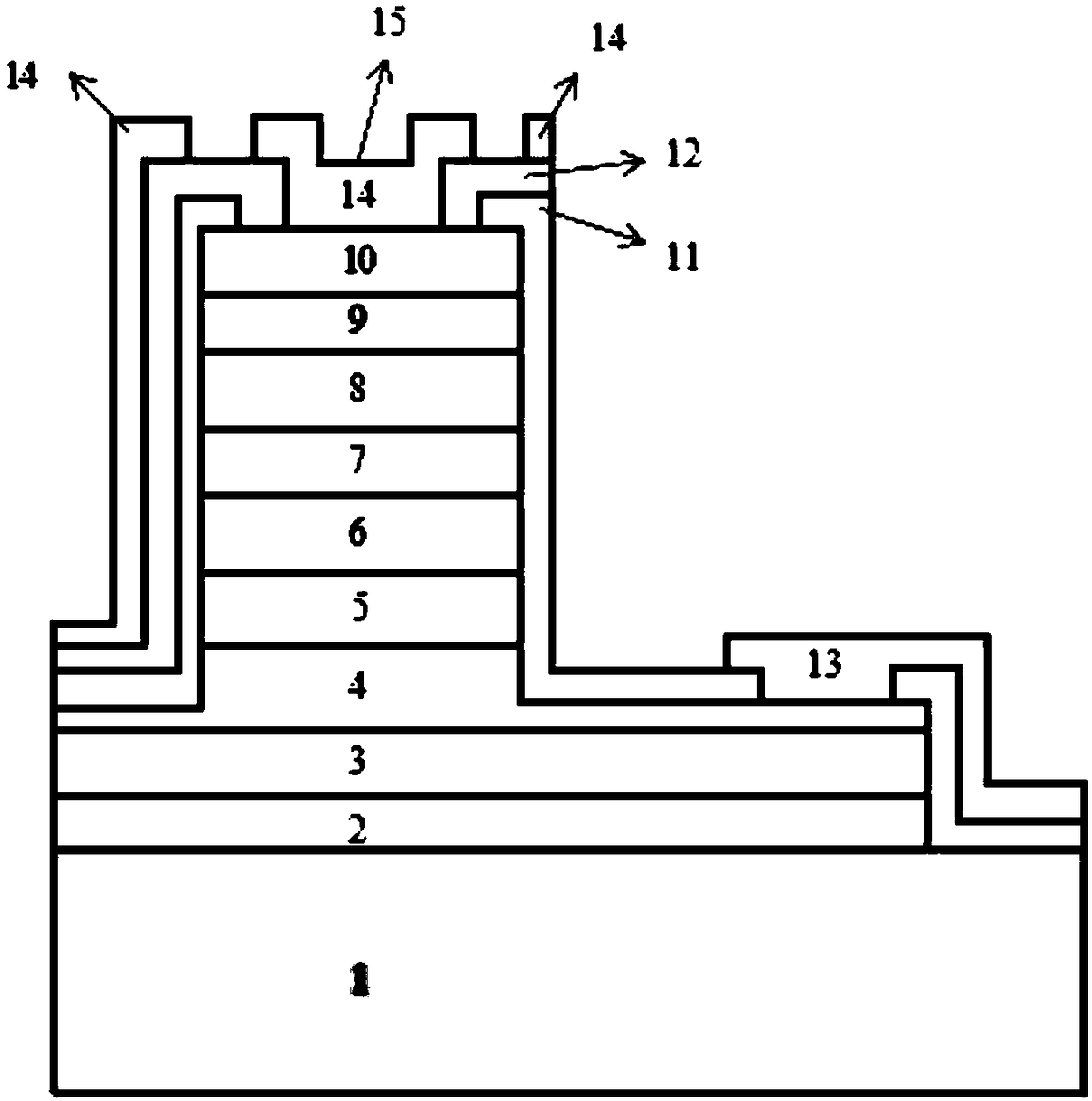
[0032] to combine figure 2 As shown, the InGaAs / InAlAs single row carrier photodetector includes: a substrate 1, a buffer layer 2 formed on the substrate 1, a sub-assembly layer 3 formed on the buffer layer 2, and a sub-assembly layer 3 formed on the The etching barrier layer 4, the build-up layer 5 formed on the etch barrier layer 4, the cliff layer 6 formed on the build-up layer 5, the conduction layer 7 formed on the cliff layer 6, the absorption layer 8 fo...


PUM


Abstract

The invention discloses a single-line carrier photodetector and a manufacturing method thereof. The photodetector includes a substrate, an epitaxial layer and an electrode, and the epitaxial layer includes an assembly layer, a cliff layer, a conduction layer, and an absorption layer stacked in sequence. and a blocking layer, the absorbing layer adopts graded doped InGaAs, the blocking layer adopts AlxIn1-xAs, 0<x<1. The present invention adopts AlxIn1-xAs material as the barrier layer and the assembly layer; the conduction layer InGaAlAs with graded composition is used to smooth the band gap between InGaAs and InAlAs, realize lattice matching, reduce the dislocation density at the heterogeneous interface and prevent electrons from The aggregation of heterogeneous interfaces accelerates the drift speed of electrons. At the same time, the doping concentration of the assembly layer presents a gradient change. On the one hand, it can effectively weaken the space charge effect, reduce the thermal power consumption of the device, and increase the saturation output current of the device; on the other hand, it can effectively weaken the speed overshoot effect and obtain a small voltage. Depends on bandwidth and better linear response.

Description

technical field [0001] The invention relates to the technical field of semiconductors, in particular to a single row carrier photodetector and a manufacturing method thereof, which can be more effectively applied to technical fields such as optical transmission systems and photon analog-to-digital conversion systems. Background technique [0002] Photodetectors are an indispensable part of optical fiber communication systems and one of the key components that determines the performance of the entire system. In large-capacity ultra-high-speed optical communication systems, people usually consider three important parameters when selecting photodetectors, namely: wide bandwidth, high efficiency and high saturated output power. For traditional PIN photodetectors, it is difficult to maintain high-speed response under high current density conditions due to the limitation of space charge effects. In order to overcome this difficulty, in 1997, T.Ishibashi et al. of NTT Photonics La...

Claims


Application Information

Patent Timeline
Patent Type & Authority Patents(China)
IPC IPC(8): H01L31/109H01L31/0304H01L31/18
CPCH01L31/03048H01L31/109H01L31/1876Y02P70/50
Inventor 王梦雪杨文献石向阳代盼谭明吴渊渊肖梦袁正兵史后明黄寓洋陆书龙
Owner SUZHOU SUNA PHOTOELECTRIC
Why Eureka
Try Eureka