An Electromagnetic Induced Potential Well Semiconductor Photoconductive Detection Device Under the Bandgap Room Temperature

An electromagnetic induction, semiconductor technology, applied in semiconductor devices, electrical components, circuits, etc., can solve problems such as low signal-to-noise ratio, complex structure, and reduced device conversion efficiency, and achieve high work efficiency, high device sensitivity, and simple device structure. compact effect

Active Publication Date: 2019-01-25
SHANGHAI INST OF TECHNICAL PHYSICS - CHINESE ACAD OF SCI
View PDF5 Cites 0 Cited by
  • Summary
  • Abstract
  • Description
  • Claims
  • Application Information

AI Technical Summary

Problems solved by technology

[0004] Aiming at the problems of long-wavelength (low-energy) photon detection, thermal noise excitation and optical excitation form a competitive mechanism, resulting in a significant drop in device conversion efficiency, low-temperature operation, complex structure, and low signal-to-noise ratio. The present invention proposes an electromagnetically induced potential well Room temperature photoconductive detection device under the semiconductor band gap, which is convenient for large-scale integration, making linear array and area array detection possible

Method used


Image

  • An Electromagnetic Induced Potential Well Semiconductor Photoconductive Detection Device Under the Bandgap Room Temperature
  • An Electromagnetic Induced Potential Well Semiconductor Photoconductive Detection Device Under the Bandgap Room Temperature

Examples


Embodiment Construction

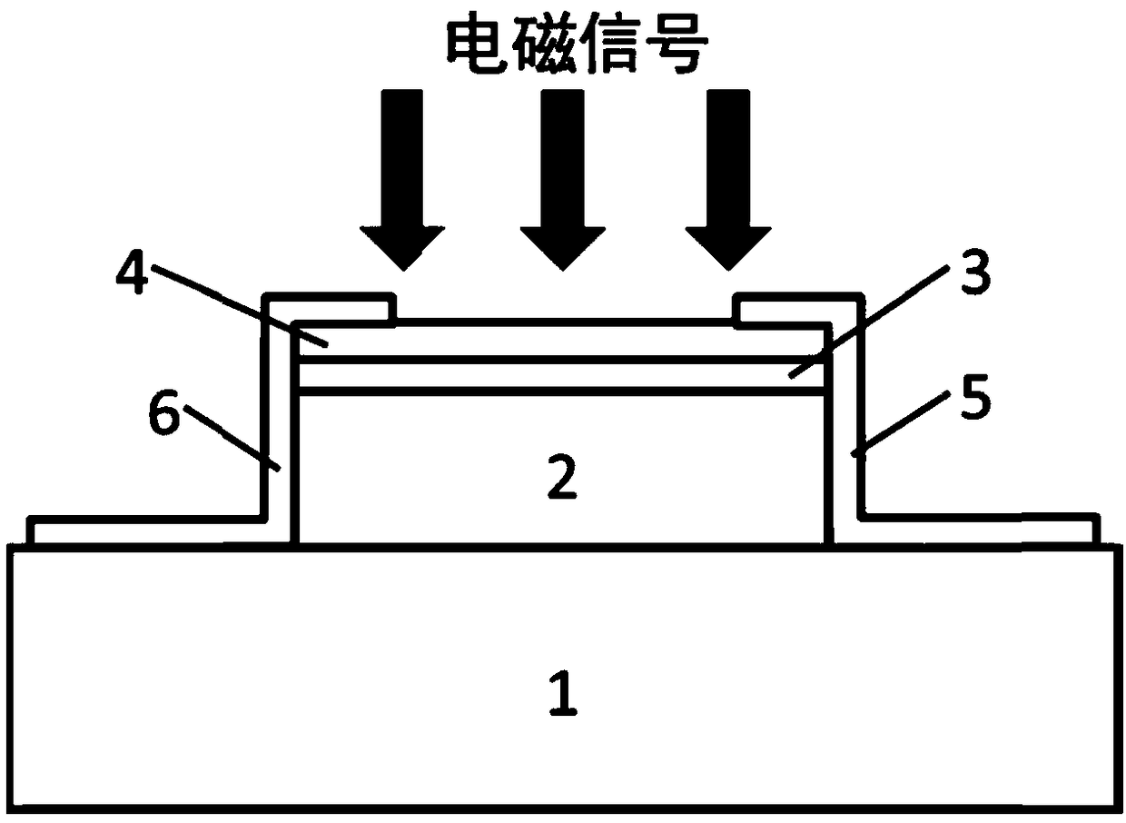
[0020] The following is attached figure 1 The present invention is further described in detail:

[0021] attached figure 1 A schematic diagram of the structure of the detector. After the electromagnetic wave signal is coupled by the metal-semiconductor-metal subwavelength structure, the electromagnetic wave antisymmetric mode induces a potential well in the semiconductor material, which binds the free carriers from the metal, thereby changing the carrier concentration in the semiconductor material , causing the resistance value of the semiconductor layer to change, the signal is connected to the preamplifier circuit through the metal wire, and the change of the resistance value of the semiconductor layer is converted into a voltage signal for amplification and reading, thereby realizing the detection of electromagnetic signals. According to attached figure 1 With the structure shown, six types of detector devices of the embodiments were fabricated.

[0022] Embodiment Dete...


PUM


Abstract

The invention discloses an electromagnetic induction potential well semiconductor forbidden room temperature light conductivity detector, the detector is formed on the semiconductor substrate from a semiconductor epitaxy, a passivation protective layer and a metal layer of the positive and negative electrode in turn. The detector is based on the electromagnetic induction potential well and remote control of lower chamber temperature and photoconductive mechanism, suitable parameter (carrier concentration, migration rate and the like) semiconductor material is selected, the reasonable detector size is designed through theory analysis, high speed optical signal to electrical signal conversion and detection are realized through the photoelectric signal being amplified and read by the pre-amplifying circuit. The device has the advantages that work can be carried out in room temperature, the stronger photoconductivity is produced in far less than the semiconductor forbidden, the sensibility is high, responding speed is fast, the structure is simple and compact, the large scale integration can be carried out and the like.

Description

technical field [0001] The invention relates to the field of photoelectric conversion devices, in particular to a room-temperature photoconductive detection device under the forbidden band of an electromagnetically induced potential well semiconductor. Background technique [0002] The conversion of optical information into electrical signals is a key foundation in the field of optoelectronic research. At present, various widely used commercial semiconductor photodetectors exhibit the advantages of high signal-to-noise ratio and fast response speed. They have shown strong appeal in applications such as optical communications, detection imaging, astronomy, biology, medicine, and non-destructive material characterization. However, there is a problem of wavelength (photon energy) selectivity in traditional photodetection: in order to excite carriers, the detected photons must have sufficient energy to excite the transition between the conduction band and the valence band, and ...

Claims


Application Information

Patent Timeline
Patent Type & Authority Patents(China)
IPC IPC(8): H01L31/115
CPCH01L31/115
Inventor 黄志明周炜姚娘娟曲越吴敬高艳卿黄敬国张飞尹一鸣褚君浩
Owner SHANGHAI INST OF TECHNICAL PHYSICS - CHINESE ACAD OF SCI
Why Eureka
Try Eureka