High-temperature quantum well super-lattice thick film thermoelectric material and production method thereof

A high-temperature quantum well, thermoelectric material technology, applied in thermoelectric device junction lead-out materials, thermoelectric device manufacturing/processing, nanotechnology for materials and surface science, etc., can solve the problem that nanowires do not have quantum wells or atoms Layer interface structure, high material cost, unsatisfactory quality and other problems, to achieve the effect of self-powered use, high thermoelectric figure of merit, and abundant reserves

Inactive Publication Date: 2017-05-31
滁州玛特智能新材料科技有限公司
View PDF6 Cites 3 Cited by
  • Summary
  • Abstract
  • Description
  • Claims
  • Application Information

AI Technical Summary

Problems solved by technology

Although the performance of these nanostructured thermoelectric materials has been improved, the cost of the synthesized materials is high and the quality is still unsatisfactory, mainly because the nanowires do not have quantum wells or atomic layer interface structures.

Method used


Image

  • High-temperature quantum well super-lattice thick film thermoelectric material and production method thereof
  • High-temperature quantum well super-lattice thick film thermoelectric material and production method thereof
  • High-temperature quantum well super-lattice thick film thermoelectric material and production method thereof

Examples


Embodiment 1

[0054] The production method of the high-temperature quantum well superlattice thick-film thermoelectric material comprises the following steps:

[0055] (1) Pulse Si gas phase precursor:

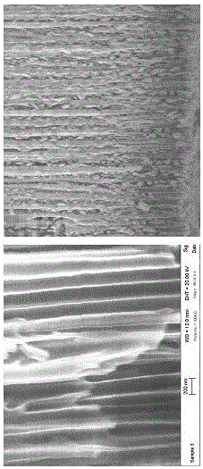
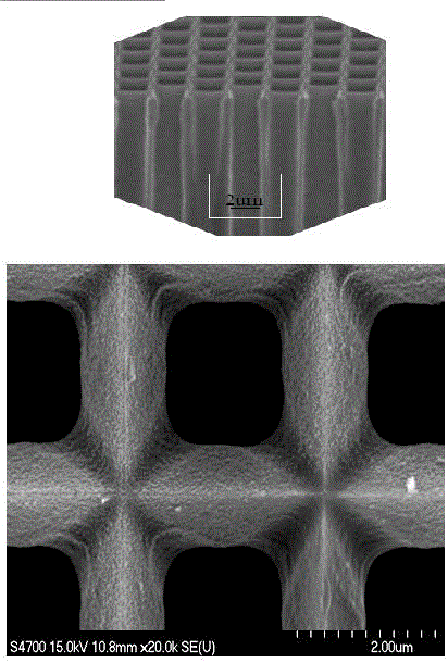
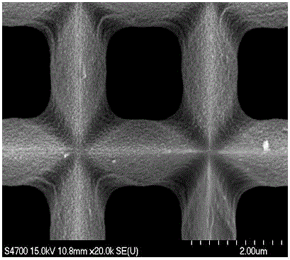
[0056] Into the reaction chamber, the Si gas phase precursor is continuously introduced, and the Si gas phase precursor is three (dimethylamino) silicon, Tris (dimethylamino) silicon, 3DMAS, 99.9999%; the substrate substrate temperature in the reaction chamber is 200 o C-400 o C; The substrate is an alumina nanoporous substrate;

[0057] (2) Clean Si gas phase precursor:

[0058] When the surface of the alumina nanoporous substrate reaches the saturation state of chemical adsorption, stop introducing the Si gas phase precursor; introduce an inert gas simultaneously to clean up the remaining Si gas phase precursor in the reaction chamber;

[0059] (3) Pulse Ge gas phase precursor:

[0060] Into the reaction chamber, the Ge gas phase precursor is continuously introduced; the Ge gas phase...

Embodiment 2

[0092] The difference between this embodiment 2 and embodiment 1 is that the substrate is a doped porous silicon template; the substrate substrate temperature in the reaction chamber is 350 o C; heating temperature of the reaction chamber: 350° C.; the same parts will not be described in detail.

Embodiment 3

[0094] The difference between this embodiment and Embodiment 2 is that the substrate is a doped silicon substrate; the temperature of the substrate in the reaction chamber is 350 o C; heating temperature of the reaction chamber: 350° C.; the same parts will not be described in detail.


PUM

PropertyMeasurementUnit
pore sizeaaaaaaaaaa
pore sizeaaaaaaaaaa
thicknessaaaaaaaaaa

Abstract

The invention discloses a production method for a high-temperature quantum well super-lattice thick film thermoelectric material. The production method comprises the following steps: growing a thermoelectric material on a porous silicon, porous aluminium oxide or doped silicon substrate through an atomic layer deposition method, wherein the thermoelectric material can grow from the inner walls of pores and then grow radially layer by layer to the centres of the pores so as to generate a thick film super-lattice thermoelectric material. A base thermoelectric material is SiGe. According to the production method for the high-temperature quantum well super-lattice thick film thermoelectric material, the super-lattice thermoelectric material which is applicable to high-temperature application is synthesized quickly through a chemical method by utilizing an atomic layer deposition method and taking a porous template as a substrate, so that high merit figure and high thermoelectric conversion efficiency are realized. The high-temperature thermoelectric material can be quickly produced on a doped or curved conductive substrate under a non-vacuum condition; the thermoelectric material has set thickness and a quantum well super-lattice structure, and is particularly suitable for high temperature, that is, the using temperature range is 700 to 1,100 DEG C.

Description

technical field [0001] The invention relates to a quantum well superlattice co-film overlay growth project in the technical field of thermoelectric materials, in particular to a quantum well superlattice thick film thermoelectric material and a production method thereof. Background technique [0002] SiGe alloy is a high-temperature thermoelectric material commonly used at present. It is often used in thermoelectric generators and is suitable for high temperatures above 700K, and its optimum operating temperature is about 1300°C. As an important high-temperature thermoelectric material, SiGe has a face-centered cubic structure and a parabolic energy band structure, and has a high Seebeck coefficient and high electrical conductivity. Therefore, the thermoelectric figure of merit is relatively high, which can reach about 0.7. Since the thermal conductivity of SiGe alloy is also higher, the ZT value of SiGe has been unable to be further improved. Recently, with the development...

Claims


Application Information

Patent Timeline
Patent Type & Authority Applications(China)
IPC IPC(8): H01L35/34H01L35/22B82Y30/00
CPCB82Y30/00H10N10/855H10N10/01
Inventor 张洪国马军涛张凯张坤
Owner 滁州玛特智能新材料科技有限公司
Why Eureka
Try Eureka