Preparation method for GaAs/Ge/GaAs heterostructure SPiN diode string used for sleeve antenna

A diode string and sleeve antenna technology, applied in the antenna, radiating element structure, semiconductor/solid-state device manufacturing and other directions, can solve the problems of low integration, incompatibility, affecting the solid-state plasma concentration, etc., to improve the injection efficiency and current, the effect of improving performance

Inactive Publication Date: 2017-06-13
XIAN CREATION KEJI CO LTD
View PDF3 Cites 6 Cited by
  • Summary
  • Abstract
  • Description
  • Claims
  • Application Information

AI Technical Summary

Problems solved by technology

[0002] At present, the materials used in SPiN diodes used in plasma reconfigurable antennas at home and abroad are all bulk silicon materials. This material has the problem of low carrier mobility in the intrinsic region, which affects the carrier concentration in the intrinsic region of the SPiN diode. Affect its solid-state plasma concentration; and the P region and N region of this structure are mostly formed by implantation process, which requires a large implant dose and energy, high requirements on equipment, and is incompatible with existing processes; and the diffusion process, Although the junction depth is deep, but at the same time, the area of ​​the P region and the N region is large, the integration degree is low, and the doping concentration is uneven, which affects the electrical performance of the SPiN diode, resulting in poor controllability of the solid-state plasma concentration and distribution.

Method used


Image

  • Preparation method for GaAs/Ge/GaAs heterostructure SPiN diode string used for sleeve antenna
  • Preparation method for GaAs/Ge/GaAs heterostructure SPiN diode string used for sleeve antenna
  • Preparation method for GaAs/Ge/GaAs heterostructure SPiN diode string used for sleeve antenna

Examples


Embodiment 1

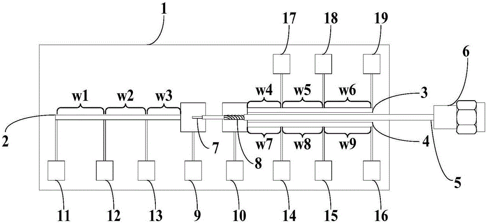
[0058] See figure 1 , figure 1 This is a schematic structural diagram of a reconfigurable sleeve antenna according to an embodiment of the present invention; the SPiN diode string is used to make a sleeve antenna, such as figure 1 As shown, the sleeve antenna includes: a semiconductor substrate (1), a SPiN diode antenna arm (2), a first SPiN diode sleeve (3), a second SPiN diode sleeve (4), a coaxial feeder (5) ), DC bias line (9, 10, 11, 12, 13, 14, 15, 16, 17, 18, 19);

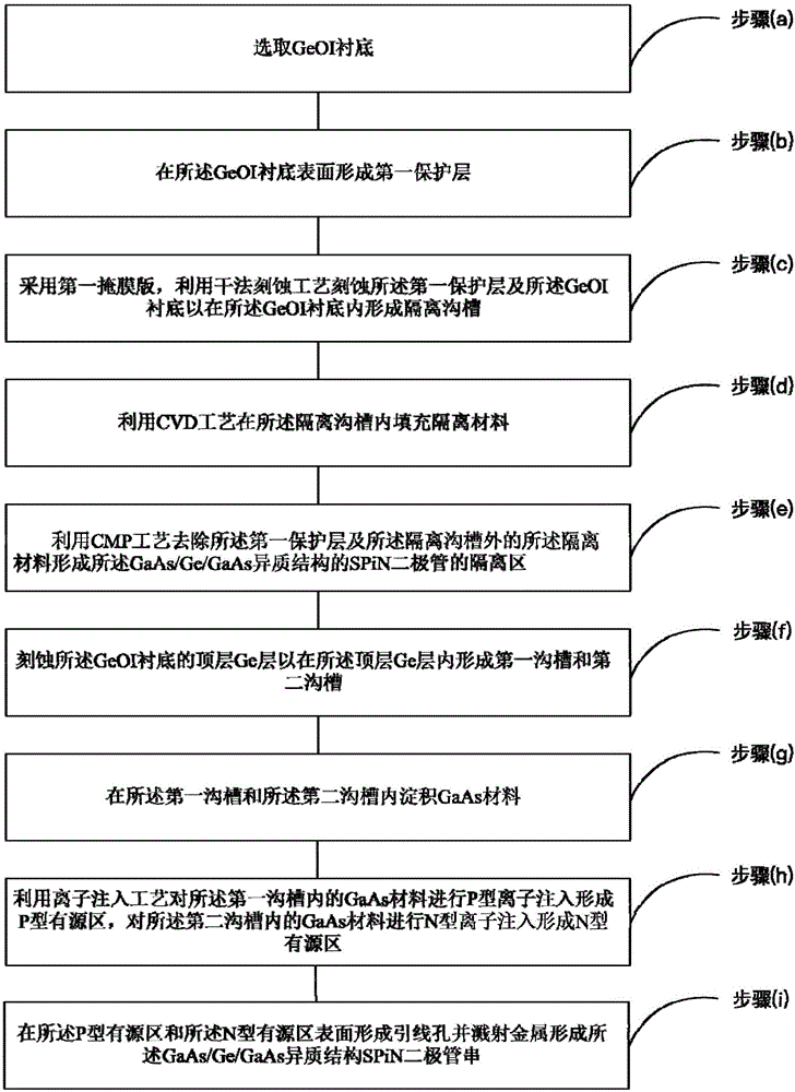
[0059] See figure 2 , figure 2 This is a flow chart of a manufacturing method of a GaAs / Ge / GaAs heterostructure SPiN diode used in a sleeve antenna according to an embodiment of the present invention. The manufacturing method includes the following steps:

[0060] (a) Select GeOI substrate;

[0061] Among them, for step (a), the reason for using GeOI substrate is that solid-state plasma antennas require good microwave characteristics, and SPiN diodes need to have good isolation characteristics and carriers that a...

Embodiment 2

[0108] See Figure 5a-Figure 5r , Figure 5a-Figure 5r This is a schematic diagram of another method for fabricating SPiN diodes with GaAs / Ge / GaAs heterostructures for sleeve antennas according to an embodiment of the present invention. Based on the above embodiment 1, the channel length is 22nm (solid plasma The SPiN diode of GaAs / Ge / GaAs heterostructure with a region length of 100 microns will be described in detail as an example. The specific steps are as follows:

[0109] Step 1, preparation steps of substrate material:

[0110] (1a) such as Figure 5a As shown, the (100) crystal orientation is selected, the doping type is p-type, and the doping concentration is 10 14 cm -3 GeOI substrate 101, the thickness of the top layer Ge is 50μm;

[0111] (1b) such as Figure 5b As shown, a chemical vapor deposition (Chemical vapor deposition, referred to as CVD) method is used to deposit a layer of first SiO with a thickness of 40 nm on a GeOI substrate 2 Layer 201;

[0112] (1c) Using chem...

Embodiment 3

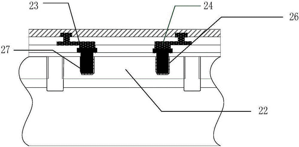
[0139] Please refer to Image 6 , Image 6 It is a schematic diagram of the device structure of another SPiN diode with GaAs / Ge / GaAs heterostructure for sleeve antenna according to an embodiment of the present invention. The SPiN diode of GaAs / Ge / GaAs heterostructure adopts the above figure 2 The manufacturing method shown is produced. Specifically, the SPiN diode of the GaAs / Ge / GaAs heterostructure is fabricated and formed on the GeOI substrate 301, and the P region 304, the N region 305 and the P region 304 of the SPiN diode are located laterally. The i regions (intrinsic regions) between the N region 305 and the N region 305 are all located in the top Ge302 of the GeOI substrate. Wherein, the SPiN diode may be isolated by STI deep trench, that is, an isolation trench 303 is provided outside the P region 304 and the N region 305, and the depth of the isolation trench 303 is greater than or equal to the thickness of the top layer Ge302.


PUM


Abstract

The invention relates to a preparation method for a GaAs/Ge/GaAs heterostructure SPiN diode string used for a sleeve antenna. The preparation method comprises the steps of (a), selecting a GeOI substrate; (b), etching a top layer Ge layer of the GeOI substrate to form a first trench and a second trench in the top layer Ge layer; (c), depositing a GaAs material in the first trench and the second trench; (d), performing P type ion implantation on the GaAs material in the first trench by adopting an ion implantation process to form a P type active region, and performing N type ion implantation on the GaAs material in the second trench to form an N type active region; and (e), forming lead holes in the surfaces of the P type active region and the N type active region and performing metal sputtering to form the GaAs/Ge/GaAs heterostructure SPiN diode. According to the embodiments, the high-performance Ge-based SPiN diode string, which is applicable to formation of a solid-state plasma antenna, can be prepared and provided through a deep trench isolation technology and the ion implantation process.

Description

Technical field [0001] The present invention relates to the technical field of integrated circuits, in particular to a method for preparing a GaAs / Ge / GaAs heterostructure SPiN diode string used in a sleeve antenna. Background technique [0002] At present, the materials used in SPiN diodes for plasma reconfigurable antennas at home and abroad are all bulk silicon materials. This material has the problem of low carrier mobility in the intrinsic region, which affects the carrier concentration in the intrinsic region of the SPiN diode. Affects its solid plasma concentration; and most of the P and N regions of the structure are formed by an implantation process. This method requires a large implant dose and energy, requires high equipment, and is incompatible with existing processes; instead, a diffusion process is used, Although the junction is deeper, at the same time, the area of ​​the P and N regions is large, the integration level is low, and the doping concentration is uneven, ...

Claims


Application Information

Patent Timeline
Patent Type & Authority Applications(China)
IPC IPC(8): H01L29/66H01L21/04H01Q23/00H01Q1/38
CPCH01L29/6609H01L21/0415H01Q1/38H01Q23/00
Inventor 左瑜张亮
Owner XIAN CREATION KEJI CO LTD
Why Eureka
Try Eureka