Growth method of N-type superlattice contact layer

A superlattice and contact layer technology, applied in electrical components, circuits, semiconductor devices, etc., can solve problems such as improving and detrimental chip luminous efficiency and reducing contact layer Schottky voltage.

Inactive Publication Date: 2017-06-16
EPITOP PHOTOELECTRIC TECH
View PDF3 Cites 1 Cited by
  • Summary
  • Abstract
  • Description
  • Claims
  • Application Information

AI Technical Summary

Problems solved by technology

However, while using P-InGaN to reduce the contact voltage, if the composition of indium IN in InGaN is too high, it will have a certain absorption effect on the light emitted by the quantum well light-emitting layer; if the composition of indium IN in InGaN is too low, then It is not conducive to reducing the Schottky voltage formed between the contact layers, and the diffusion effect of P-InGaN on current is poor, which is not conducive to the improvement of the luminous efficiency of the entire chip

Method used


Image

  • Growth method of N-type superlattice contact layer
  • Growth method of N-type superlattice contact layer

Examples


Embodiment 1

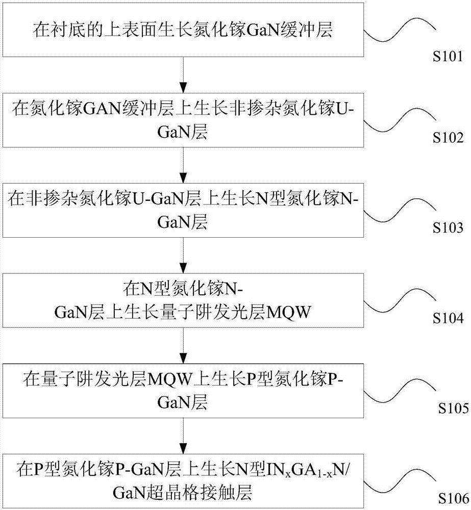
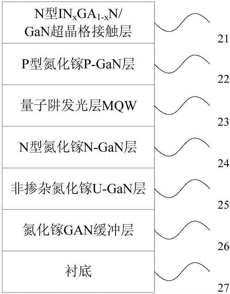
[0037]The N-type IN x GA 1-x The N / GaN superlattice contact layer is N-type (IN 0.15 GA 0.85 N / GaN) 3 Superlattice contact layer, N-type (IN 0.15 GA 0.85 N / GaN) 3 The thickness of the superlattice contact layer is 15 nm, where IN 0.15 GA 0.85 The thickness of N super is 2 nm, the thickness of GaN is 3 nm, the SiH 4 The dopant rubs at a concentration of 1.2 x 10e 21 cm -3 .

[0038] And the growth method of the N-type INGAN / GAN superlattice contact layer is described in detail, the method includes:

[0039] 1. Put the sapphire (Patterned Sapphire Substrate, PSS for short) substrate 21 into the reaction chamber, the flow ratio of N2:H2:NH3 is (0:120:0) liters per minute (Standard Liter per Minute, SLM for short), The pressure of the reaction chamber is 500 Torr, the temperature is raised to 1070° C., and stabilized for 300 seconds, and the substrate 21 is purified at high temperature.

[0040] 2. Lower the temperature to 550° C., the flow ratio of N2:H2:NH3 is (75:1...

Embodiment 2

[0047] The N-type IN x GA 1-x The N / GaN superlattice contact layer is N-type (IN 0.1 GA 0.9 N / GaN) 4 Superlattice contact layer, N-type (IN 0.1 GA 0.9 N / GaN) 4 The thickness of the superlattice contact layer is 16 nm, where N-type IN 0.1 GA 0.9 The thickness of N is 2 nm, the thickness of GaN is 2 nm, the SiH 4 The dopant rubs at a concentration of 1.9×10e 20 cm -3 -1.2×10e 21 cm -3 between.

[0048] 1. Put the sapphire (Patterned Sapphire Substrate, PSS for short) substrate 21 into the reaction chamber, the flow ratio of N2:H2:NH3 is (0:120:0) liters per minute (Standard Liter per Minute, SLM for short), The pressure of the reaction chamber is 500 Torr, the temperature is raised to 1080° C., and stabilized for 300 seconds, and the substrate is purified at high temperature.

[0049] 2. Lower the temperature to 550° C., the flow ratio of N2:H2:NH3 is (75:150:56) SLM, the pressure of the reaction chamber is controlled at 500 Torr, and a low-temperature GaN buffer l...


PUM

PropertyMeasurementUnit
thicknessaaaaaaaaaa
thicknessaaaaaaaaaa
thicknessaaaaaaaaaa

Abstract

The embodiment of the invention provides a growth method of an N-type superlattice contact layer. The growth method comprises the steps that a gallium nitride GaN buffer layer is grown on the upper surface of a substrate; an undoped gallium nitride U-GaN layer is grown on the gallium nitride GAN buffer layer; an N-type gallium nitride N-GaN layer is grown on the undoped gallium nitride U-GaN layer; a quantum well luminescent layer MQW is grown on the N-type gallium nitride N-GaN layer; a P-type gallium nitride P-GaN layer is grown on the quantum well luminescent layer MQW; and an N-type INxGA1-xN / GaN superlattice contact layer is grown on the P-type gallium nitride P-GaN layer, wherein x is greater than or equal to 0 and less than 1. The Schottky barrier between a metal electrode and an epitaxial wafer can be reduced by the unique electrical characteristics so that uniformity of current injection can be enhanced, the brightness can be enhanced, junction temperature between an electrode wire and the surface of the metal electrode can be reduced, and the probability of high current core granule breakdown can also be reduced.

Description

technical field [0001] The invention relates to the technical field of semiconductor lighting, in particular to a growth method of an N-type superlattice contact layer. Background technique [0002] In the process of making the electrodes of light-emitting diodes, in order to reduce the contact voltage between the surface of the epitaxial layer and the metal, special materials and processes are generally used to grow the contact layer to ensure the voltage generated by the contact between the metal and the non-metal due to the potential barrier. The traditional manufacturing process is to grow a layer of P-type indium gallium nitride P-InGaN on the basis of the P-type layer to reduce the Schottky voltage formed by the contact barrier. However, while using P-InGaN to reduce the contact voltage, if the composition of indium IN in InGaN is too high, it will have a certain absorption effect on the light emitted by the quantum well light-emitting layer; if the composition of indi...

Claims


Application Information

Patent Timeline
Patent Type & Authority Applications(China)
IPC IPC(8): H01L33/40H01L33/00
CPCH01L33/40H01L33/007H01L2933/0016
Inventor 焦建军黄小辉周德保康建梁旭东
Owner EPITOP PHOTOELECTRIC TECH
Why Eureka
Try Eureka