InGaN/GaN LED nanosecond pulse driving circuit

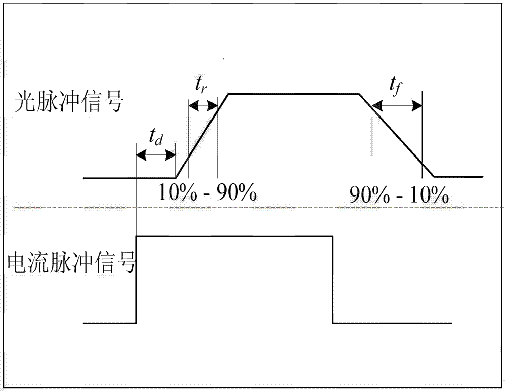
A drive circuit and nanosecond pulse technology, which is applied in the field of InGaN/GaNLED nanosecond pulse drive circuits, can solve the problems of shortening the rise time and fall time of optical pulse signals, so as to improve transient response time, reduce fall time, shorten The effect of rise time

Active Publication Date: 2017-06-20
SHAANXI NORMAL UNIV
View PDF3 Cites 2 Cited by
  • Summary
  • Abstract
  • Description
  • Claims
  • Application Information

AI Technical Summary

Problems solved by technology

[0018] The above methods all involve the use of current pulses to drive LEDs, but they do not use a better method to effectively improve the response rate of LEDs and effectively shorten the rise time and fall time of optical pulse signals.

Method used


Image

  • InGaN/GaN LED nanosecond pulse driving circuit
  • InGaN/GaN LED nanosecond pulse driving circuit
  • InGaN/GaN LED nanosecond pulse driving circuit

Examples


Embodiment Construction

[0044] The following will clearly and completely describe the technical solutions in the embodiments of the present invention with reference to the accompanying drawings in the embodiments of the present invention. Obviously, the described embodiments are only part of the embodiments of the present invention, not all of them. Based on the embodiments of the present invention, all other embodiments obtained by persons of ordinary skill in the art without making creative efforts belong to the protection scope of the present invention.

[0045] The present invention will be further described below in conjunction with the accompanying drawings.

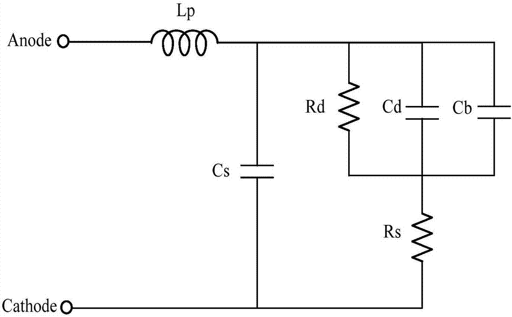
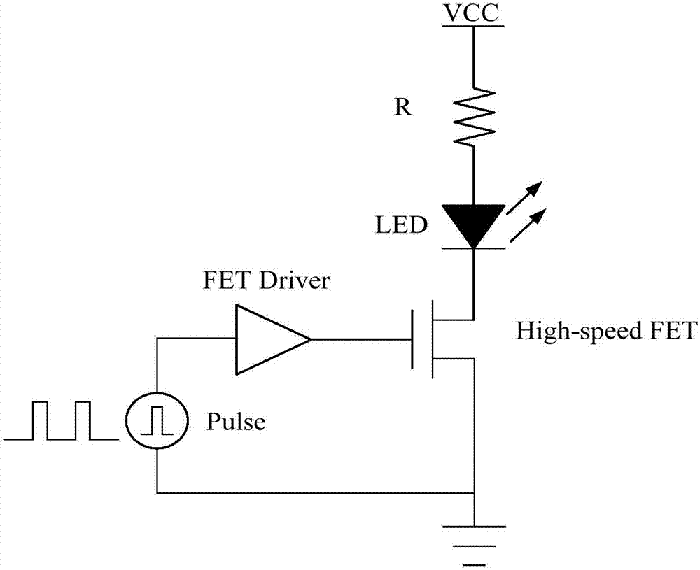
[0046] Such as Figure 5 An InGaN / GaN LED nanosecond pulse drive circuit shown includes a high-impedance drive circuit for high-speed field effect transistors, a switch circuit for high-speed field effect transistors, a pulse signal generation module, Schottky diodes SBD1 and SBD2, and a first inductor L1, capacitor C;

[0047] The puls...


PUM


Abstract

The invention discloses an InGaN / GaN LED nanosecond pulse driving circuit. Through a current pulse peak technology, a loop composed of Schottky diodes SBD1 and SBD2 and a capacitor C produces a current peak, and the rise time of light pulse is shortened by a few nanoseconds. Thus, the rise time of light pulse is shortened. A first inductor L1 is connected between the cathode of an LED and a bias power supply Vcc. In the phase of current pulse fall, an undershoot current is produced through a reverse current loop provided by the inductor. Thus, the fall time of light pulse is reduced, the LED goes out more quickly, and the fall time of light pulse is improved greatly. A high-speed field effect transistor switching circuit quickly charges the parasitic output capacitor of a main switch by increasing auxiliary switches, so that the closing time of the main switch is shortened, and the switching rate of field effect transistors is increased. The anode of the LED is connected with a DC bias voltage Vcc, so that an equivalent capacitor can be fully charged before the arrival of current pulse. Therefore, the switch-on delay of the LED is shortened effectively, and the transient response time of the LED is improved greatly.

Description

[0001] 【Technical field】 [0002] The invention relates to an LED driving circuit, in particular to an InGaN / GaN LED nanosecond pulse driving circuit. [0003] 【Background technique】 [0004] In recent years, with the continuous research on the preparation technology, growth process and device packaging technology of group III elements and nitrogen compound semiconductor materials, optoelectronic semiconductor devices have developed rapidly, especially the heterojunction and multiple quantum wells composed of InGaN / GaN Breakthroughs have been made in the research of structured light-emitting materials, and high-brightness blue and green light-emitting diodes (Lighting-emitting Diode, LED), short-wavelength lasers, and avalanche photodiode detectors have been successfully prepared. Based on the special base material and quantum well structure of InGaN / GaN, on the one hand, it passivates the surface of the LED, reduces the loss caused by the recombination of carriers injected int...

Claims


Application Information

Patent Timeline
Patent Type & Authority Applications(China)
IPC IPC(8): H05B33/08H05B44/00
CPCH05B45/37Y02B20/30
Inventor 辛云宏贺帆马剑飞
Owner SHAANXI NORMAL UNIV
Why Eureka
Try Eureka