
Epitaxial structure for improving light output power of ultraviolet LED

A technology of epitaxial structure and light output, applied in the field of ultraviolet LED, to achieve the effect of improving electron blocking efficiency, high radiation recombination rate, and reducing electron leakage

Pending Publication Date: 2017-07-07
GUANGDONG UNIV OF TECH
View PDF7 Cites 6 Cited by
  • Summary
  • Abstract
  • Description
  • Claims
  • Application Information

AI Technical Summary

Problems solved by technology

[0004] The purpose of the present invention is to propose an epitaxial structure to improve the output power of ultraviolet LEDs, the purpose is to improve the crystal quality of ultraviolet LED chips, optimize the electron blocking effect of the electron blocking layer, reduce electron leakage, thereby improving the efficiency of ultraviolet LED devices. , to increase the optical output power

Method used


Image

  • Epitaxial structure for improving light output power of ultraviolet LED

Examples


Embodiment 1

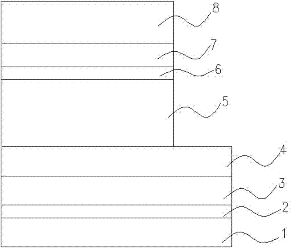
[0027] like figure 1 As shown, an epitaxial structure for improving the output power of ultraviolet LED light, including the structure from bottom to top: substrate 1, GaN buffer layer 2, undoped GaN layer 3, doped N-type GaN layer 4, AlGaN / GaN multiple quantum well structure 5 , an insertion layer 6 , an electron blocking layer EBL7 , and a P-type GaN layer 8 .

[0028] like figure 1 As shown, the substrate 1 is a sapphire substrate. A 25nm GaN buffer layer 2 is grown on a sapphire substrate. Next, a 2.5 μm undoped u-GaN layer is grown on the GaN buffer layer 2 . Then, grow an N-type GaN layer with a thickness of 3 μm on the 2.5 μm undoped u-GaN layer with a Si doping concentration of 5×10 18 cm -3 . Subsequently, on the N-type GaN layer, an AlGaN / GaN multi-quantum well structure 5 is grown, and the specific composition is 6 alternating periods of Al 0.15 Ga 0.85 N / GaN multiple quantum well structure, where Al 0.15 Ga 0.85 The thickness of each layer of N is 10nm, ...


PUM

PropertyMeasurementUnit
Thicknessaaaaaaaaaa
Growth temperatureaaaaaaaaaa
Thicknessaaaaaaaaaa

Abstract

The invention discloses an epitaxial structure for improving light output power of an ultraviolet LED. The epitaxial structure comprises a substrate, a GaN buffer layer, a non-doped GaN layer, a doped N-type GaN layer, a AlGaN / GaN multi-quantum well structure, an insertion layer, an electron barrier layer EBL and a P-type GaN layer which are sequentially arranged from bottom to top, wherein the substrate employs a sapphire substrate, the thickness of the GaN buffer layer is 20-25 nanometers, the growth temperature of the GaN buffer layer is 530-550 DEG C, the GaN buffer layer is recrystallized under heat preservation for 6 minutes at 1,050 DEG C, the thickness of the non-doped GaN layer is 2.0-2.5 micrometers, the growth temperature of the non-doped GaN layer is 1,050 DEG C, the thickness of the doped N-type GaN layer is 2.5-3.0 micrometers, the Si doping concentration is 5*10<18>cm<-3>, the growth temperature is 1,050 DEG C, and the multi-quantum well AlGaN / GaN structure is formed by alternatively growing multi-quantum well AlGaN layers and multi-quantum well GaN layers according to six periods. By improving the crystal quality of an ultraviolet LED chip, the electron barrier effect of the electron barrier layer is optimized, the electron leakage is reduced, so that the efficiency reduction of an ultraviolet LED device is improved, and the light output power is improved.

Description

technical field [0001] The invention belongs to the field of ultraviolet LEDs. Specifically, it improves the crystal quality of ultraviolet LED chips by designing a new epitaxial structure, optimizes the electron blocking effect of the electron blocking layer, reduces electron leakage, and improves the efficiency of ultraviolet LED devices. Optical output power. Background technique [0002] In the UV-A region in the ultraviolet light-emitting band, the light-emitting wavelength is usually between 320nm and 400nm. The ultraviolet light in this band is used in many aspects, such as ultraviolet curing, currency identification, artificial sunlight, air purification and lighting. At this stage, there are many problems in the production process level of ultraviolet LEDs, especially UV-B with a wavelength range of 275nm-320nm, and UV-C with a wavelength range of 100nm-275nm. The technology is higher and the production is more difficult. Therefore, ultraviolet LEDs in the UV-A ba...

Claims


Application Information

Patent Timeline
IPC IPC(8): H01L33/14H01L33/32
CPCH01L33/145H01L33/32
Inventor 何苗黄波熊德平杨思攀周海亮
Owner GUANGDONG UNIV OF TECH
Learn More