

Semiconductor device, manufacturing method of the semiconductor device, and electronic device
A technology for semiconductors and devices, applied in the fields of electronic devices, semiconductor devices and preparation methods, can solve the problems of low product yield, unfavorable production costs, device failures, etc., to reduce source-drain contact resistance, save production costs, and avoid circuit failures Effect
- Summary
- Abstract
- Description
- Claims
- Application Information
AI Technical Summary
Problems solved by technology
Method used
Image

Examples
Embodiment 1
[0045] Attached below Figures 1a-1h The method for preparing the semiconductor device of the present invention is further described.
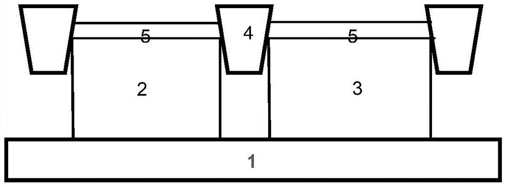
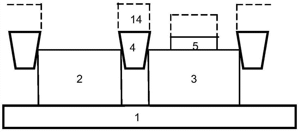
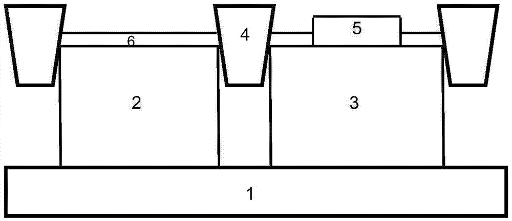
[0046] First, step 101 is performed to provide a semiconductor substrate 1 , the semiconductor substrate 1 includes a high-voltage device region 3 and a low-voltage device region 2 , and a patterned high-voltage gate oxide layer 5 is formed on the high-voltage device region.
[0047] Specifically, such as Figure 1a Said, in this step, the semiconductor substrate 1 can be at least one of the materials mentioned below: silicon, silicon-on-insulator (SOI), silicon-on-insulator (SSOI), silicon-germanium-on-insulator (S-SiGeOI), silicon germanium on insulator (SiGeOI) and germanium on insulator (GeOI), etc.
[0048] In this embodiment, the material of the semiconductor substrate 1 is preferably silicon.
[0049] The semiconductor substrate 1 includes a high-voltage device region 3 and a low-voltage device region 2, a high-voltage well region and...
Embodiment 2
[0094] The present invention also provides a semiconductor device prepared by the method described in Embodiment 1. The device includes a semiconductor substrate 1, and the semiconductor substrate 1 includes a high-voltage device region 3 and a low-voltage device region 2. In the high-voltage A patterned high voltage gate oxide layer 5 is formed on the device region.
[0095] The semiconductor substrate 1 may be at least one of the materials mentioned below: silicon, silicon-on-insulator (SOI), silicon-on-insulator (SSOI), silicon-germanium-on-insulator (S-SiGeOI), insulator Silicon germanium-on-insulator (SiGeOI) and germanium-on-insulator (GeOI), etc.
[0096] In this embodiment, the material of the semiconductor substrate 1 is preferably silicon.
[0097] The semiconductor substrate 1 includes a high-voltage device region 3 and a low-voltage device region 2, a high-voltage well region and a low-voltage well region are formed in the semiconductor substrate, and isolation is...
Embodiment 3
[0106] An embodiment of the present invention provides an electronic device, which includes the semiconductor device prepared by the method of Embodiment 1.
[0107] The electronic device may be selected from a personal computer, a game machine, a cellular phone, a personal digital assistant, a video camera, a digital camera, etc., but is not limited to the above-listed devices.
PUM
| Property | Measurement | Unit |
|---|---|---|
| Thickness | aaaaa | aaaaa |
| Thickness | aaaaa | aaaaa |
| Thickness | aaaaa | aaaaa |
Abstract
Description
Claims
Application Information