A nanowire transistor based on resonant tunneling and its preparation method

A resonant tunneling and nanowire technology, which is applied in semiconductor/solid-state device manufacturing, semiconductor devices, electrical components, etc., can solve problems such as difficulty in meeting the requirements of smaller technology nodes, nanowire transistors that have not been reported, and increased static power consumption. , to achieve low requirements for ion implantation process and annealing process, reduce sub-threshold slope, and facilitate popularization and application

Inactive Publication Date: 2021-02-02
INST OF SEMICONDUCTORS - CHINESE ACAD OF SCI
View PDF2 Cites 0 Cited by
  • Summary
  • Abstract
  • Description
  • Claims
  • Application Information

AI Technical Summary

Problems solved by technology

However, for conventional junction-free silicon nanowire transistors, its transport nature is still consistent with that of traditional MOSFETs, and its subthreshold slope is greater than 60mV / decade, and the off-state current of junction-free transistors is larger than that of traditional MOSFETs, increasing the Static power
[0004] Because tunneling transistors rely on quantum tunneling for transport, they can achieve very small off-state currents and sub-threshold slopes less than 60mV / decade. However, tunneling transistors are mostly realized by structural design, and the structure is complex, which is difficult to meet the requirements of smaller technology nodes. Require
Therefore, if the advantages of the two can be combined, a device with better performance can be prepared with a simpler process, which is of great research value, but nanowire transistors based on tunneling have not yet been reported.

Method used


Image

  • A nanowire transistor based on resonant tunneling and its preparation method
  • A nanowire transistor based on resonant tunneling and its preparation method
  • A nanowire transistor based on resonant tunneling and its preparation method

Examples


Embodiment Construction

[0041] In order to make the object, technical solution and advantages of the present invention clearer, the present invention will be described in further detail below in conjunction with specific embodiments and with reference to the accompanying drawings.

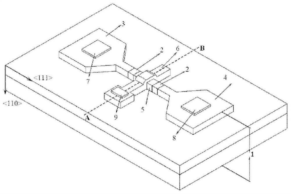
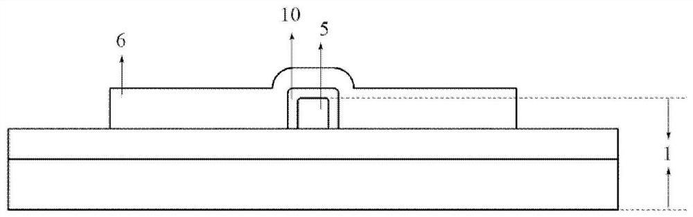
[0042] Such as figure 1 as shown, figure 1 is a three-dimensional schematic diagram of a nanowire transistor based on resonant tunneling according to an embodiment of the present invention, figure 2 It is a nanowire transistor based on resonant tunneling according to an embodiment of the present invention in figure 1 The cross-sectional view taken along the line AB. combine figure 1 and figure 2 As shown, the nanowire transistor includes: SOI substrate 1 except for the source region 3, the drain region 4, the part of the nanowire 5, the double barrier structure 2, the source region 3, the drain region 4, the nanowire 5, the gate electrode 6, source electrode 7, drain electrode 8, gate electrode 9 and insulating die...


PUM

PropertyMeasurementUnit
thicknessaaaaaaaaaa
thicknessaaaaaaaaaa
thicknessaaaaaaaaaa

Abstract

The invention discloses a nanowire transistor based on resonance tunneling. The nanowire transistor comprises an SOI substrate, a tunneling barrier structure, a source region, a drain region, nanowires, a grid electrode, a source electrode, a drain electrode, a grid electrode and an insulating dielectric layer. The tunneling barrier structure is located on the buried oxide layer of the SOI substrate. The source region, the drain region and the nanowire are formed by etching top silicon of the SOI substrate; the nanowire is positioned between the source region and the drain region; wherein thesource region, the drain region and the nanowire are not directly connected and are connected through a tunneling barrier structure, the insulating dielectric layer is formed on the surfaces of the source region, the drain region and the nanowire, the grid electrode is formed on the insulating dielectric layer above the nanowire, the source electrode is formed on the source region, the drain electrode is formed on the drain region, and the grid electrode is formed on the grid electrode. According to the nanowire transistor structure based on resonance tunneling and the preparation method of the nanowire transistor structure, the sub-threshold slope is reduced, and large conduction current and small source-drain contact resistance can be achieved.

Description

technical field [0001] The invention relates to the technical field of manufacturing semiconductor devices, in particular to a nanowire transistor based on resonant tunneling and a preparation method thereof. Background technique [0002] With the continuous advancement of integrated circuit manufacturing technology, the size of metal oxide semiconductor field effect transistor (MOSFET) devices continues to shrink, and the current MOSFET technology node has entered 7nm. If the size of the device is to be further reduced, it is necessary to overcome many challenges in the principle and process of the device, such as the short channel effect and the fabrication of the PN junction. [0003] The preparation process of the junction-free silicon nanowire transistor is simple, and its source, drain, and channel regions are uniformly doped, and no junction is required to relieve the pressure caused by ion implantation and annealing in the ultra-steep junction. At the same time, the...

Claims


Application Information

Patent Timeline
Patent Type & Authority Patents(China)
IPC IPC(8): H01L29/778H01L21/265H01L21/335
CPCH01L21/26513H01L29/66431H01L29/778
Inventor 赵晓松韩伟华郭仰岩窦亚梅张晓迪吴歆宇杨富华
Owner INST OF SEMICONDUCTORS - CHINESE ACAD OF SCI
Why Eureka
Try Eureka