Manufacturing method of vertical device with GaN epitaxial layer growing on silicon substrate

A manufacturing method and epitaxial layer technology, applied in semiconductor/solid-state device manufacturing, semiconductor devices, electrical components, etc.

Active Publication Date: 2017-07-21
M MOS SEMICON HK
View PDF4 Cites 4 Cited by
  • Summary
  • Abstract
  • Description
  • Claims
  • Application Information

AI Technical Summary

Problems solved by technology

[0015] The current commercial epitaxial silicon nitride structure grown on silicon single crystals, the sequence of epitaxial layers on the surface of silicon single crystals is a layer of aluminum nitride (AlN) with a thickness of several hundred nanometers, a layer of about several microns Thick AlGaN, a layer of GaN with a thickness of several microns, then a buffer layer of silicon nitride with a thickness of several hundred nanometers, followed by AlGaN with a thickness of about 25 nanometers, forming a two-dimensional electron gas (2DEG) between AlGaN and GaN. The structure can only be used as a device for the preparation of lateral structures

Method used


Image

  • Manufacturing method of vertical device with GaN epitaxial layer growing on silicon substrate
  • Manufacturing method of vertical device with GaN epitaxial layer growing on silicon substrate
  • Manufacturing method of vertical device with GaN epitaxial layer growing on silicon substrate

Examples


Embodiment Construction

[0065] The preferred embodiments of the present invention will be described below in conjunction with the accompanying drawings. It should be understood that the preferred embodiments described here are only used to illustrate and explain the present invention, and are not intended to limit the present invention.

[0066] figure 2 According to the flow chart of the manufacturing method of vertical GaN-based Schottky diode semiconductor device of the present invention, reference will be made below figure 2 , the method for manufacturing the vertical GaN-based Schottky diode semiconductor device of the present invention is described in detail.

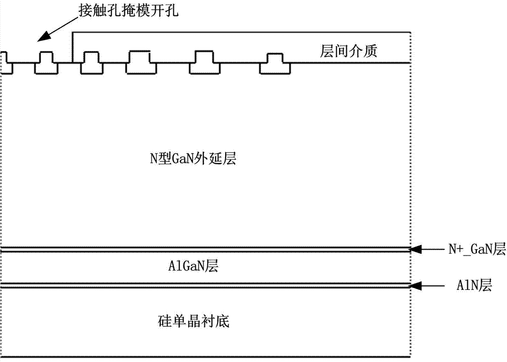
[0067] First, in step 201, an AlN layer, an AlGaN layer, a high electron concentration N-type GaN epitaxial layer (N+_GaN layer), and a low electron concentration N-type GaN epitaxial layer (N type epitaxial layer) are sequentially grown on a silicon single crystal substrate And P type GaN epitaxial layer (P type epitaxial layer). F...


PUM

PropertyMeasurementUnit
thicknessaaaaaaaaaa
thicknessaaaaaaaaaa
thicknessaaaaaaaaaa

Abstract

Provided is a manufacturing method of a vertical device with a GaN epitaxial layer growing on a silicon substrate. The method includes following steps: growing an AlN layer, an AlGaN layer, an N+_GaN layer, an N-type GaN epitaxial layer, and a P-type GaN epitaxial layer on a silicon single-crystal substrate in sequence; etching the P-type GaN epitaxial layer to form grooves; injecting silicon-ion N-type doping agent to convert a P-type region to an N-type region; forming an interlayer dielectric at the outermost surface of the epitaxial layer, and forming contact hole mask opening pores in the interlayer dielectric; forming an emitting region metal cushion layer and a terminal region field plate; thinning the silicon single-crystal silicon substrate, and perforating the back surface of the silicon substrate; etching a silicon surface exposed by the silicon substrate to form deep grooves; and filling in the grooves with metal, and metalizing the back surface of the silicon single-crystal substrate as a back electrode of the device. According to the manufacturing method of the vertical device, the device dimension and the manufacturing cost are reduced, and the device with the vertical structure can provide higher and more effective power and better cost performance.

Description

technical field [0001] The invention relates to a method for manufacturing a gallium nitride semiconductor device, in particular to a method for manufacturing a vertical gallium nitride-based vertical device. Background technique [0002] The third-generation semiconductor materials include: cadmium sulfide (CdS), zinc oxide (ZnO), silicon carbide (SiC), gallium nitride (GaN), diamond, etc. The bandgap of these semiconductor materials is greater than 2.2eV. In terms of electronic devices, the research on SiC and GaN is relatively mature, and it is currently a hot spot in the field of semiconductor materials and device research in the world. [0003] The GaN band gap is 3.4eV. The wide band gap enables GaN materials to withstand higher operating temperatures, and also enables GaN materials to have a larger breakdown electric field. A larger breakdown electric field means that the device can withstand higher operating voltages. , can improve the power characteristics of the d...

Claims


Application Information

Patent Timeline
Patent Type & Authority Applications(China)
IPC IPC(8): H01L21/336H01L29/872
CPCH01L29/66143H01L29/66462H01L29/8725
Inventor 欧阳伟伦梁安杰罗文健
Owner M MOS SEMICON HK
Why Eureka
Try Eureka