Integrated full perovskite solar energy cell and LED display system and manufacturing method thereof

A technology of solar cells and integrated systems, applied in circuits, photovoltaic power generation, electrical components, etc., can solve the problems of single crystal silicon time-consuming and energy-consuming, complex production process, and high difficulty in commercial application

Inactive Publication Date: 2017-07-25
SHANGHAI UNIV
View PDF3 Cites 4 Cited by
  • Summary
  • Abstract
  • Description
  • Claims
  • Application Information

AI Technical Summary

Problems solved by technology

However, monocrystalline silicon consumes time and energy, high cost, complex production process, and environmental pollution during the production process, which limits its large-scale use.
Although the second-generation solar cells save materials and have low growth costs, they also have unavoidable shortcomings. Te, In, Ga, etc. are elements with little reserves on the earth, and they are more scarce than Au, which will make them unable to be mass-produced , greatly affecting its output value
The third-generation solar cells, such as organic photovoltaics (OPVs), dye-sensitized solar cells (DSCs) and quantum dot solar cells (QDSCs), are solution-coated on unconventional substrates by processes such as blade coating, Shiscreen printing, and spray coating. So as to ensure low-cost solar cell power generation, but relatively unstable
In terms of efficiency, the EQE reached above 8% for the first time at the end of last year, and this year at least two 2DPeLED EQEs have reached above 8%, but the preparation process is complicated and commercial application is difficult

Method used


Image

  • Integrated full perovskite solar energy cell and LED display system and manufacturing method thereof
  • Integrated full perovskite solar energy cell and LED display system and manufacturing method thereof
  • Integrated full perovskite solar energy cell and LED display system and manufacturing method thereof

Examples


Embodiment 1

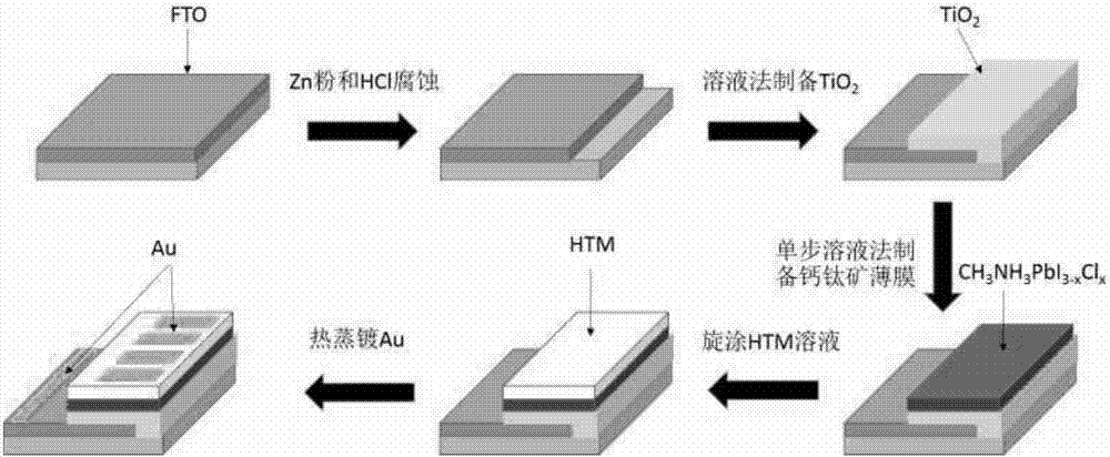
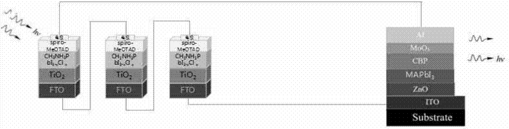
[0053] In this embodiment, see image 3 with Figure 4 , An all-perovskite solar cell and LED display integrated system, characterized in that: the solar cell 1 and the LED display device 2 are assembled to form an integrated system, and the solar cell 1 is a solar cell device using a planar perovskite film, The LED display device 2 uses a perovskite film as the luminescent material layer, and connects the anode of the perovskite solar cell 1 and the cathode of the LED display device 2 in series through wires, and connects the cathode substrate of the perovskite solar cell 1 and The anode substrates of the LED display device 2 are connected in series to form a closed loop. The solar cell 1 absorbs solar energy and emits electric energy to supply power to the LED display device 2.

[0054] In this embodiment, see image 3 The solar cell 1 sequentially consists of an anode substrate, a titanium dioxide window layer, a perovskite film layer, a hole transport layer film and a cathode ...

Embodiment 2

[0087] This embodiment is basically the same as the first embodiment, and the special features are:

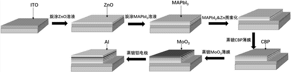
[0088] In this embodiment, in an all-perovskite solar cell and LED display integrated system, a hole blocking layer is also provided between the light-emitting layer of the perovskite film and the hole transport layer of the CBP film.

[0089] In this embodiment, when the LED display device is prepared in step b of preparing an all-perovskite solar cell and LED display integrated system, and MAPbI is prepared in step (c) of step ⑶ 3 After the film is deposited, the substrate device prepared in step (c) is then transferred to the multi-source vapor deposition system, and the chamber pressure of the multi-source vapor deposition system is controlled to be 5x10- 3 Pa, adjust the temperature of the corresponding evaporation source, make the TPBI material reach the sublimation point, and deposit on MAPbI in gaseous state 3 On the film, a dense TPBI film is formed as a hole blocking layer,...


PUM


Abstract

The invention discloses an integrated full perovskite solar energy cell and LED display system and a manufacturing method thereof. A single step solution method is employed to grow a MAPbI3-xClx film, through leads, an anode of a perovskite solar energy cell is connected in series with a cathode of an LED display device, a cathode substrate of the perovskite solar energy cell is connected in series with an anode substrate of the LED display device, a closed loop is formed, solar energy is absorbed by the solar energy cell, electric energy is then emitted to supply power for the LED display device, integrated spin coating manufacturing of the solar energy cell and the LED display device is accomplished, and the full perovskite system is realized. Raw materials are relatively easy to get, the raw materials are saved, and the manufacturing operation has better economic effects The method is further advantaged in that the perovskite solar energy cell and the LED display with high-efficiency are manufactured, integration is lastly carried out, operation is simple, production line manufacturing is convenient, the materials are saved, time and energy are saved, and large-scale production is easy.

Description

Technical field [0001] The invention relates to an LED display system and a preparation method thereof, in particular to a solar cell and LED display integrated system and a preparation method thereof, and is applied to the technical field of photoelectric device preparation. Background technique [0002] With the increasing global energy consumption and environmental destruction, traditional fossil energy can hardly meet the needs of human economic and social sustainable development. Therefore, people are always looking for clean and renewable energy. At present, a variety of new energy sources are continuously being used and developed, such as solar energy, water energy, wind energy and so on. Among them, solar energy has become the most promising renewable energy source due to its endless sources and stability. How to use solar energy efficiently and at low cost has always attracted people's attention. At present, there are two main types of using solar energy: photothermal...

Claims


Application Information

Patent Timeline
Patent Type & Authority Applications(China)
IPC IPC(8): H01L27/32H01L51/56
CPCH10K59/60H10K71/164H10K71/00Y02E10/549Y02P70/50
Inventor 崔四维刘风采焦钰清黄霏王浩然倪超伟蔡江张新月徐闰杨绪勇
Owner SHANGHAI UNIV
Why Eureka
Try Eureka