Method and device for precise and controllable cutting of graphene ribbons by photocatalytic oxidation
A technology of photocatalytic oxidation and graphene tape, which is applied in metal processing and other directions, can solve problems such as human injury, expensive equipment, and complicated operating conditions, and achieve the effect of avoiding equipment corrosion
- Summary
- Abstract
- Description
- Claims
- Application Information
AI Technical Summary
Problems solved by technology
Method used
Image
Examples
Embodiment 1
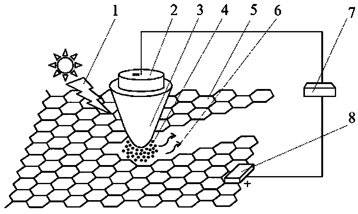
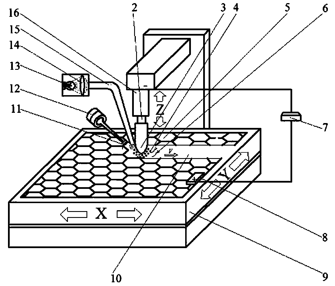
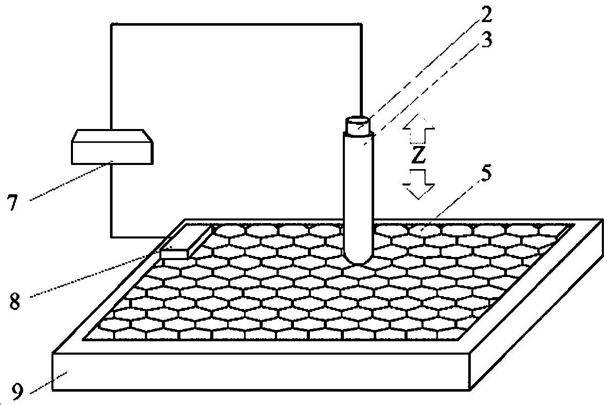
[0037] Step 1: fixing the graphene 5 with the substrate on the two-dimensional micro-motion stage 9 driven by piezoelectric ceramics, the two-dimensional micro-motion stage 9 is nanoscale;
[0038] Step 2: Use the magnetostrictive mechanism 16 and the power controller 7 to realize the Z-direction positioning of the semiconductor probe 3. The material of the outer layer of the semiconductor probe 3 is titanium dioxide, the material of the metal core 2 of the inner layer is titanium, and the outer layer of the semiconductor probe 3 is titanium dioxide. The diameter size is 20nm, and the lower end is smoothly transitioned;
[0039] Step 3: Use atomizer 12 to make the mass percentage 0.5%H 2 o 2 The auxiliary liquid 11 mixed with 99.5% deionized water is atomized, and the atomized auxiliary liquid 11 is adsorbed on the surface of the semiconductor probe 3;
[0040] Step 4: The ultraviolet light source 13 emits ultraviolet light 1, which is focused by the condenser lens 14 and ir...
Embodiment 2
[0045] Step 1: fixing the graphene 5 with the substrate on the two-dimensional micro-motion stage 9 driven by piezoelectric ceramics, the two-dimensional micro-motion stage 9 is nanoscale;
[0046] Step 2: Use the magnetostrictive mechanism 16 and the power controller 7 to realize the Z-direction positioning of the semiconductor probe 3. The material of the outer layer of the semiconductor probe 3 is zinc oxide, the material of the metal core 2 of the inner layer is zinc, and the material of the semiconductor probe 3 is zinc oxide. The outer diameter is 50nm, with a smooth transition at the lower end;
[0047] Step 3: use the atomizer 12 to atomize the auxiliary liquid 11 formed by mixing 1% Fenton reagent and 99% deionized water by mass percentage, and the atomized auxiliary liquid 11 is adsorbed on the surface of the semiconductor probe 3;
[0048] Step 4: The ultraviolet light source 13 emits ultraviolet light 1, which is focused by the condenser lens 14 and irradiated on t...
Embodiment 3
[0053] Step 1: fixing the graphene 5 with the substrate on the two-dimensional micro-motion stage 9 driven by piezoelectric ceramics, the two-dimensional micro-motion stage 9 is nanoscale;
[0054] Step 2: Use the magnetostrictive mechanism 16 and the power controller 7 to realize the Z-direction positioning of the semiconductor probe 3. The material of the outer layer of the semiconductor probe 3 is zirconium dioxide, and the material of the metal core 2 of the inner layer is zirconium. 3 The outer diameter is 100nm, and the lower end is smoothly transitioned;
[0055] Step 3: Use atomizer 12 to make the mass percentage 12%K 2 FeO 4 The auxiliary liquid 11 mixed with 88% deionized water is atomized, and the atomized auxiliary liquid 11 is adsorbed on the surface of the semiconductor probe 3;
[0056] Step 4: The ultraviolet light source 13 emits ultraviolet light 1, which is focused by the condenser lens 14 and irradiated on the semiconductor probe 3 by the light source tra...
PUM
 Abstract
Description
Claims
Application Information


