
Method for preparing silicon epitaxial wafer for step recovery diode

A technology for recovering diodes and silicon epitaxial wafers, used in chemical instruments and methods, semiconductor/solid-state device manufacturing, crystal growth, etc.

Active Publication Date: 2017-08-04
CHINA ELECTRONICS TECH GRP NO 46 RES INST
View PDF6 Cites 11 Cited by
  • Summary
  • Abstract
  • Description
  • Claims
  • Application Information

AI Technical Summary

Problems solved by technology

At present, there is still a large gap between the width of the transition zone of domestic silicon epitaxial wafers and similar foreign products. The percentage range of the width of the transition zone to the thickness of the epitaxial layer generally ranges from 15% to 20%, which cannot meet the device index requirements.

Method used


Image

  • Method for preparing silicon epitaxial wafer for step recovery diode
  • Method for preparing silicon epitaxial wafer for step recovery diode
  • Method for preparing silicon epitaxial wafer for step recovery diode

Examples


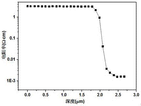
Embodiment 1

[0023] (1) First use hydrogen chloride (HCl) gas with a purity ≥ 99.99% to etch the graphite base of the epitaxial furnace to completely remove the residual deposited substances on the base, set the etching temperature to 1130°C, and set the HCl gas flow rate to was 3 L / min, and the HCl etching time was set to 3 min. Immediately after the etching is completed, a layer of undoped polysilicon is re-grown on the surface of the base, and the growth material is SiHCl 3 , the flow rate is set to 15 L / min, and the time is set to 10 min.

[0024] (2) Load the silicon single crystal substrate into the pit of the base of the epitaxial furnace, and use nitrogen and hydrogen with a purity of ≥99.999% to purge the reaction chamber of the epitaxial furnace in sequence. The gas flow rate is set to 300 L / min, and the purge time is for 10 min.

[0025] (3) The surface of the silicon single crystal substrate was polished with HCl, the HCl flow rate was set to 1 L / min, the polishing temperatur...

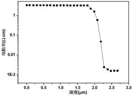
Embodiment 2

[0034] (1) First use hydrogen chloride (HCl) gas with a purity ≥ 99.99% to etch the graphite base of the epitaxial furnace to completely remove the residual deposited substances on the base, set the etching temperature to 1130°C, and set the HCl gas flow rate to was 1 L / min, and the HCl etching time was set to 3 min. Immediately after the etching is completed, a layer of undoped polysilicon is re-grown on the surface of the base, and the growth material is SiHCl 3 , the flow rate is set to 14 L / min, and the time is set to 12 min.

[0035] (2) Load the silicon single crystal substrate into the pit of the base of the epitaxial furnace, and use nitrogen and hydrogen with a purity of ≥99.999% to purge the reaction chamber of the epitaxial furnace in sequence. The gas flow rate is set to 300 L / min, and the purge time is for 12 min.

[0036] (3) The surface of the silicon single crystal substrate was polished with HCl, the HCl flow rate was set to 1 L / min, the polishing temperatur...

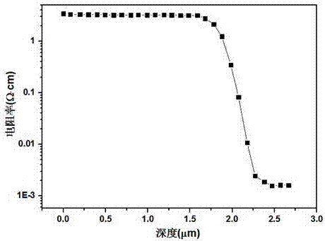
Embodiment 3

[0045] (1) First use hydrogen chloride (HCl) gas with a purity of ≥99.99% to etch the base of the epitaxial furnace to completely remove the residual deposits on the base, set the etching temperature to 1130°C, and set the HCl gas flow rate to 3 L / min, HCl etching time is set to 3 min. Immediately after the etching is completed, a layer of undoped polysilicon is re-grown on the surface of the base, and the growth material is SiHCl 3 , the flow rate was set at 15 L / min, and the growth time was set at 10 min.

[0046] (2) Load the silicon single crystal substrate into the pit of the base of the epitaxial furnace, and use nitrogen and hydrogen with a purity of ≥99.999% to purge the chamber in sequence. The gas flow rate is set to 300 L / min, and the purge time is 10 min. .

[0047] (3) The surface of the silicon single crystal substrate was polished with HCl, the HCl flow rate was set to 1 L / min, the polishing temperature was set to 1130 °C, and the polishing time was set to 3 m...


PUM

PropertyMeasurementUnit
thicknessaaaaaaaaaa
thicknessaaaaaaaaaa
thicknessaaaaaaaaaa

Abstract

The invention discloses a method for preparing a silicon epitaxial wafer for a step recovery diode. According to the preparation method, the problem in the conventional silicon epitaxial wafer process for the step recovery diode that the width of a transition area cannot be controlled is solved. A two-section growth manner is adopted in the epitaxial layer growth process, purging is performed for a period of time by using hydrogen with repeatedly changeable flow, impurities are continuously diluted and discharged out of a reaction chamber of an epitaxial furnace, and the first section of the epitaxial layer grows at a low temperature and a low speed, so that the gas phase self-doping influence is reduced, the structure of the transition area is improved, and then purging is performed for a period of time again by using the hydrogen with the repeatedly changeable flow, the second section of the epitaxial layer rapidly grows at a high temperature, and finally, the target thickness and electrical resistivity are achieved. Due to the optimized epitaxial process, control of substrate impurity self-diffusion factors under a normal pressure is realized, and the width of the transition area is narrowed, so that the width accounts for 13-15% of the thickness percentage of the epitaxial layer, and the use requirement of the step recovery diode is met.

Description

technical field [0001] The invention relates to the preparation technology of semiconductor epitaxial materials, in particular to a preparation method of silicon epitaxial wafers for step recovery diodes. Background technique [0002] Step recovery diodes are referred to as step tubes for short. They have the characteristics of forward voltage drop and high reverse breakdown voltage, and their drop time is extremely short, and their forward conductivity is also very good. The step tube is very special in transient response, its fall time is close to 0, and the current changes rapidly when it is turned off. Taking advantage of its excellent volt-ampere characteristics, step tubes are mainly used in frequency multiplication circuits, ultra-high-speed pulse shaping and generation circuits. [0003] The characteristics of the step tube are based on the special distribution of impurities in the PN junction. Its structural feature is that it has a steep impurity distribution area...

Claims


Application Information

Patent Timeline
Patent Type & Authority Applications(China)
IPC IPC(8): C30B25/20C30B29/06H01L21/02
CPCC30B25/186C30B25/20C30B29/06H01L21/02381H01L21/02532H01L21/0262
Inventor 李明达陈涛薛兵李普生
Owner CHINA ELECTRONICS TECH GRP NO 46 RES INST
Learn More