Method for improving thermal conductivity of gallium oxide material

A technology of gallium oxide and two-dimensional materials, which is applied in the field of improving the thermal conductivity of gallium oxide materials, can solve the problems of high thermal conductivity, no thermal conductivity, low carrier mobility, etc., to improve thermal conductivity and facilitate promotion, high value effect

Active Publication Date: 2017-08-11
INST OF MICROELECTRONICS CHINESE ACAD OF SCI
View PDF9 Cites 7 Cited by
  • Summary
  • Abstract
  • Description
  • Claims
  • Application Information

AI Technical Summary

Problems solved by technology

[0003] Gallium oxide material has a bandgap width as high as 4.8eV, its breakdown field strength is about three times that of 4H-SiC and GaN, and its preparation cost is low, so it has become a potential stock in the field of high-power devices. However, due to gallium oxide The material has low carrier mobility and very low thermal conductivity compared to other semiconductor materials, which limits its application in high-power devices
[0004] However, high-power devices have higher requirements for thermal c

Method used


Image

  • Method for improving thermal conductivity of gallium oxide material
  • Method for improving thermal conductivity of gallium oxide material
  • Method for improving thermal conductivity of gallium oxide material

Examples


Embodiment Construction

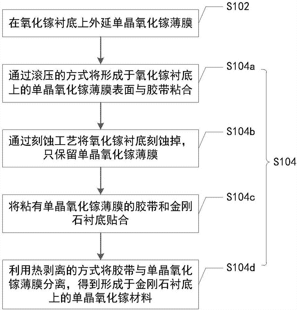
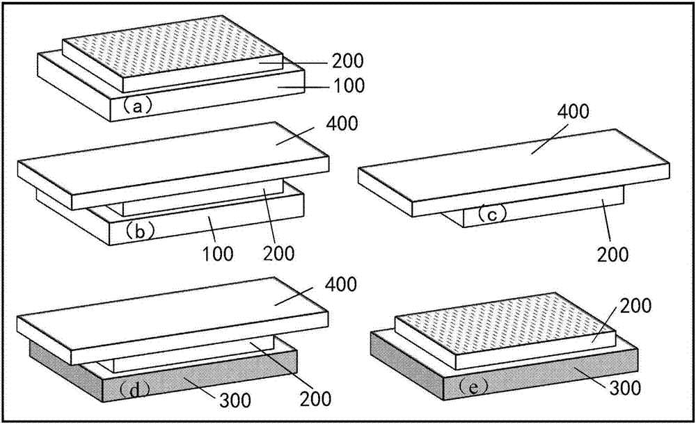
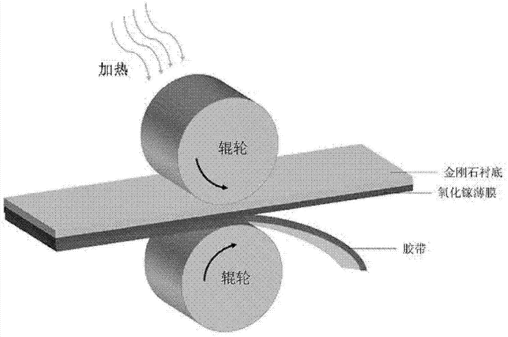
[0025] The invention provides a method for improving the thermal conductivity of gallium oxide materials, using an etching process combined with a two-dimensional material transfer method to transfer a single crystal gallium oxide film to a substrate with a thermal conductivity greater than 200W / m·K and compatible with semiconductors In terms of materials, a single crystal gallium oxide material formed on the above substrate is obtained, which effectively improves the thermal conductivity of the gallium oxide material. The present invention aims at improving the thermal conductivity of gallium oxide, and at the same time facilitates its use in the field of semiconductor device production, ensuring that gallium oxide materials are used in semiconductor devices, so the availability of gallium oxide materials must be ensured on the basis of improving thermal conductivity , so as to promote its application promotion.

[0026] In order to make the object, technical solution and adv...


PUM

PropertyMeasurementUnit
Thermal conductivityaaaaaaaaaa
Roughnessaaaaaaaaaa
Thicknessaaaaaaaaaa

Abstract

The invention provides a method for improving thermal conductivity of a gallium oxide material. The method comprises: an epitaxial monocrystalline gallium oxide film is grown on a gallium oxide substrate; the monocrystalline gallium oxide film is transferred to a substrate material which has a thermal conductivity of more than 200 W/m.K and is compatible with semiconductors by means of an etching process combined with two-dimensional material transfer, and a monocrystalline gallium oxide material formed on the substrate is obtained. By transferring the monocrystalline gallium oxide film to a substrate which has a thermal conductivity of more than 200 W/m.K and is compatible with semiconductors, including diamond, an AlN substrate, a GaN substrate, a SiC substrate or a composite substrate composed of a Si substrate and diamond deposited on the Si substrate, the thermal conductivity of the gallium oxide material is effectively improved; and the process of dry transfer technique is simple, more mature process can be formed easily, thus the method is easy to promote, facilitates improving the production quality, and has high value for practical use.

Description

technical field [0001] The invention belongs to the technical field of semiconductors, in particular to a method for improving the thermal conductivity of gallium oxide materials. Background technique [0002] With the continuous development of information technology and electronic power systems, the market demand for wide bandgap semiconductors is increasing. The first generation semiconductor materials Si, Ge, the second generation semiconductor materials GaAs, InP, and the third generation semiconductor materials SiC , the continuous popularization and development of GaN has played a key role in new energy, smart grid, electric vehicles, high-speed trains and other life fields as well as radar, aerospace and other military fields. [0003] Gallium oxide material has a bandgap width as high as 4.8eV, its breakdown field strength is about three times that of 4H-SiC and GaN, and its preparation cost is low, so it has become a potential stock in the field of high-power device...

Claims


Application Information

Patent Timeline
IPC IPC(8): H01L21/02H01L21/683H01L23/373
CPCH01L21/02565H01L21/02664H01L21/6836H01L23/3738H01L2221/68386
Inventor 龙世兵何启鸣董航刘琦吕杭炳刘明
Owner INST OF MICROELECTRONICS CHINESE ACAD OF SCI
Why Eureka
Try Eureka