P-type crystalline silicon cell structure and manufacturing method thereof

A crystalline silicon battery and battery technology, applied in the field of solar cells, can solve the problems of battery leakage and component packaging problems that have not been solved well, and have not been applied on a large scale, so as to achieve good battery performance, reduce light shading area, and improve the operation process. simple effect

Inactive Publication Date: 2017-08-15
滁州隆基乐叶光伏科技有限公司
View PDF8 Cites 2 Cited by
  • Summary
  • Abstract
  • Description
  • Claims
  • Application Information

AI Technical Summary

Problems solved by technology

However, the leakage of MWT batteries and the packaging of components have not been well resolved, which makes MWT, as the core technology for improving the battery front, has not been applied on a large scale.

Method used


Image

  • P-type crystalline silicon cell structure and manufacturing method thereof
  • P-type crystalline silicon cell structure and manufacturing method thereof
  • P-type crystalline silicon cell structure and manufacturing method thereof

Examples


Embodiment 1

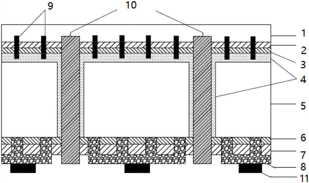
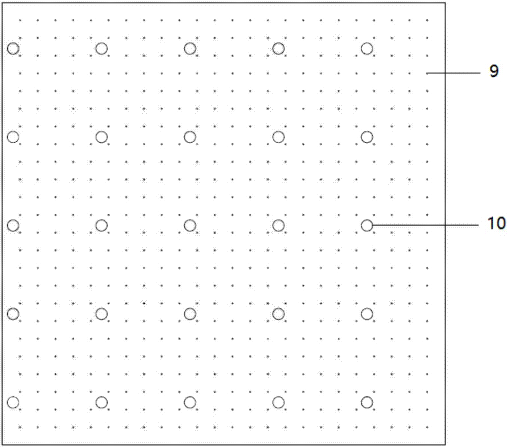
[0052] (1) A laser is used to form 5×5 equally spaced through holes on a P-type monocrystalline silicon wafer, and the diameter of a single through hole is 500um.

[0053] (2) Anisotropically etch the P-type monocrystalline silicon wafers with through holes in a KOH solution at about 80°C to obtain a surface pyramid structure.

[0054] (3) Use POCl3 as the dopant for low-pressure diffusion at 800-900°C to form an N-type layer on the front surface of the silicon wafer and the surface layer of the through-hole wall, and the square resistance after doping is 75Ω / □.

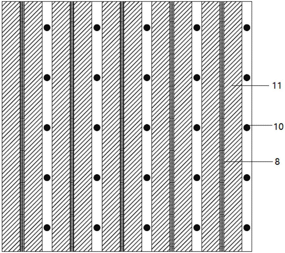
[0055] (4) Using inkjet method to spray wax on the through hole and its surrounding area.

[0056] (5) Use wet etching to remove the phosphosilicate glass, back knots and paraffin wax on the front side of the silicon wafer.

[0057] (6) The etched silicon wafer is annealed in an annealing furnace at 650° C., and a dense thermal silicon oxide is grown on the surface of the silicon wafer.

[0058] (7) A PECVD method was used to d...

Embodiment 2

[0064] (1) A laser is used to form 6×6 equally spaced through holes on the P-type polysilicon wafer, and the diameter of a single through hole is 400um.

[0065] (2) Put the P-type polycrystalline silicon wafers with through holes in a dry plasma texturing equipment to obtain a polymorphic micro-nano structure, and then perform surface modification in a BOE solution.

[0066] (3) Using PH3 as an impurity, doping with ion implantation, forming an N-type layer on the front surface of the silicon wafer and the surface layer of the through-hole wall, the square resistance after doping is 80Ω / □.

[0067] (4) Using inkjet method to spray wax on the through hole and its surrounding area.

[0068] (5) Use wet etching to remove the phosphosilicate glass, back knots and paraffin wax on the front side of the silicon wafer.

[0069] (6) The ALD method is used to deposit 20nm of aluminum oxide and 60nm of silicon nitride on the back of the silicon wafer; the ALD method is used to deposit 20nm of sil...


PUM

PropertyMeasurementUnit
Widthaaaaaaaaaa
Line widthaaaaaaaaaa
Lengthaaaaaaaaaa

Abstract

The invention provides a P-type crystalline silicon cell structure and a manufacturing method thereof. The P-type crystalline silicon cell structure sequentially comprises a transparent conductive thin film, partial metal electrodes, a front-side antireflection film, a front-side passivation film, N-type doped layers, P-type crystalline silicon substrates, a first back-side passivation film, a second back-side passivation film, partial back surface fields and back-side positive electrodes from the front side to the back side, wherein the transparent conductive thin film and the partial metal electrodes on the front side of a cell are in contact to conduct collected electrons transversely, and introduce the electrons into a negative electrode region on the back side of the cell by means of via electrodes penetrating the cell panel; and the back-side positive electrodes and the partial back surface fields on the back side of the cell are distributed in regions outside the via electrodes, and the partial back surface fields are connected with the back-side positive electrodes. The P-type crystalline silicon cell structure and the manufacturing method thereof greatly enhance the degree of fusion with the existing module packaging process, improve the conversion efficiency of the module, and simplifies the process.

Description

Technical field [0001] The invention belongs to the technical field of solar cells, and particularly relates to a P-type crystalline silicon cell structure and a manufacturing method thereof. Background technique [0002] In recent years, due to the development and application of new energy technologies, the structure of crystalline silicon solar cells has been extensively studied, the conversion efficiency has been continuously improved, and the production cost has continued to decrease. At present, crystalline silicon solar cells account for more than 90% of the total global solar cell market. The conversion efficiency of crystalline silicon cell production lines has exceeded 21%. The annual global installed capacity is about 70GW and the growth rate is obvious, which is comparable to thermal power generation. The electricity cost gap is narrowing and is expected to remain flat in the next few years. As a kind of clean energy, crystalline silicon solar cells play an increasing...

Claims


Application Information

Patent Timeline
IPC IPC(8): H01L31/0224H01L31/18
CPCH01L31/022425H01L31/022441H01L31/18H01L31/1884Y02P70/50
Inventor 沈玉婷赵科雄
Owner 滁州隆基乐叶光伏科技有限公司
Why Eureka
Try Eureka