Low-noise high-sensitivity global pixel unit structure and formation method thereof

A pixel unit, high-sensitivity technology, applied in the field of image sensors, can solve the problems of MOS capacitor capacitance value limitation, storage signal distortion, affecting charge signal, etc., to achieve the effect of increasing storage capacitance value, reducing readout noise, and increasing effective area

Active Publication Date: 2017-09-22
SHANGHAI INTEGRATED CIRCUIT RES & DEV CENT +1
View PDF4 Cites 6 Cited by
  • Summary
  • Abstract
  • Description
  • Claims
  • Application Information

AI Technical Summary

Problems solved by technology

like figure 2 As shown, incident light with a certain incident angle is only reflected on the metal isolation 101 used to prevent crosstalk between pixel units (as indicated by the dotted arrow pointing upwards in the figure), since the peripheral area of ​​the lower plate of the capacitor is silicon substrate, and the silicon substrate is light-transmissive, so some light will still pass through the silicon substrate and enter the lower plate of the storage capacitor, that is, the MOS capacitor, affecting the charge signal stored on the MOS capacitor, resulting in distortion of the stored signal
[0013] In addition, since the lower plate 104 of the MOS capacitor and the photodiode 102 for the pixel unit to receive light are located in the silicon substrate 103 of the first chip, in order to ensure the sensitivity of the pixel unit, we hope to increase the area of ​​the photosensitive area, that is, the photodiode as much as possible. , so the area of ​​the MOS capacitor is limited by the photodiode, that is, the capacitance value of the MOS capacitor is limited, that is, the readout noise of the pixel unit cannot be effectively reduced
At the same time, the area of ​​the photodiode is also limited by the lower plate of the capacitor. The part of the silicon substrate occupied by the lower plate cannot be used for light sensing, which affects the sensitivity of the pixel unit.

Method used


Image

  • Low-noise high-sensitivity global pixel unit structure and formation method thereof
  • Low-noise high-sensitivity global pixel unit structure and formation method thereof
  • Low-noise high-sensitivity global pixel unit structure and formation method thereof

Examples


Embodiment Construction

[0058] The specific embodiments of the present invention will be further described in detail below with reference to the accompanying drawings.

[0059] It should be noted that in the following specific embodiments, when the embodiments of the present invention are described in detail, in order to clearly show the structure of the present invention for ease of description, the structure in the drawings is not drawn according to the general scale. Partial enlargement, deformation, and simplification of processing have been implemented. Therefore, this should be avoided as a limitation of the present invention.

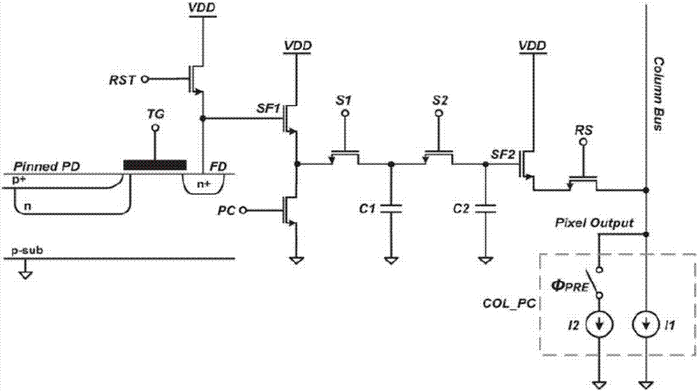
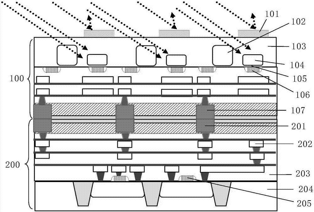
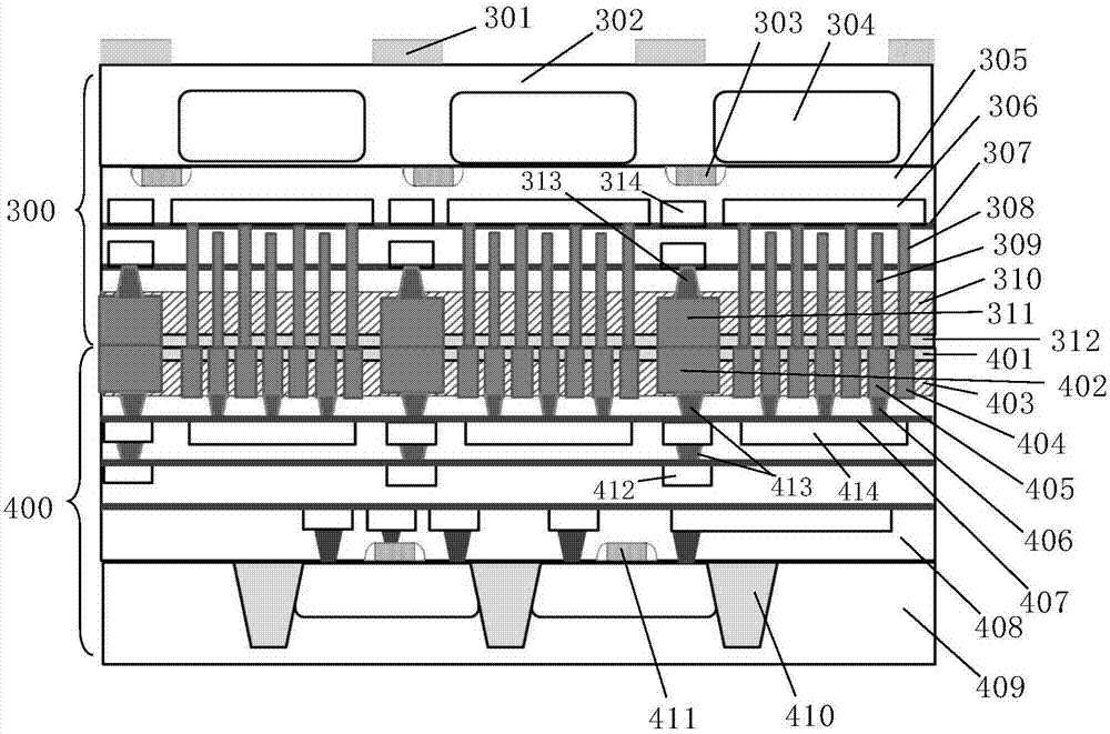
[0060] In the following specific embodiments of the present invention, please refer to image 3 , image 3 It is a schematic structural diagram of a global pixel unit with low noise and high sensitivity according to a preferred embodiment of the present invention. Such as image 3 As shown, a low-noise and high-sensitivity global pixel unit structure of the present invention...


PUM


Abstract

The invention discloses a low-noise high-sensitivity global pixel unit structure and a formation method thereof. Through forming a vertical capacitor structure in stacked first-chip and second-chip rear-channel dielectric layers, an original MOS capacitor which is located in a first chip silicon substrate is replaced so that an effective area of the capacitor can be greatly increased, a storage capacitance value of a global exposure pixel unit is increased too and a reading-out noise is effectively reduced. Simultaneously, a lightproof capacitor lower pole plate extraction is arranged above upper and lower pole plates of the capacitor and is used as a shading structure so that incident light passing through a silicon substrate and the rear-channel dielectric layers can be prevented from impacting on a capacitor storage signal. Besides, because a MOS capacitor structure does not need to be formed in the first chip silicon substrate, a photosensitive area of a photodiode can be increased to a position occupied by the MOS capacitor originally so that sensitivity of the pixel unit is increased.

Description

Technical field [0001] The invention relates to the field of image sensors, in particular to a structure of a global exposure pixel unit of a low-noise high-sensitivity stacked CMOS image sensor and a forming method thereof. Background technique [0002] An image sensor refers to a device that converts light signals into electrical signals. Generally, large-scale commercial image sensor chips include charge-coupled devices (CCD) and complementary metal oxide semiconductor (CMOS) image sensor chips. [0003] Compared with traditional CCD sensors, CMOS image sensors have the characteristics of low power consumption, low cost, and compatibility with CMOS technology, so they are more and more widely used. Now CMOS image sensors are not only used in consumer electronics fields such as micro digital cameras (DSC), cell phone cameras, camcorders, and digital single-lens reflex (DSLR), but also in automotive electronics, surveillance, biotechnology, and medicine. [0004] In order to monito...

Claims


Application Information

Patent Timeline
Patent Type & Authority Applications(China)
IPC IPC(8): H01L27/146H04N5/374
CPCH01L27/14603H01L27/14609H01L27/1461H01L27/1464H01L27/14643H01L27/14683H04N25/76
Inventor 赵宇航顾学强周伟王言虹范春晖
Owner SHANGHAI INTEGRATED CIRCUIT RES & DEV CENT
Why Eureka
Try Eureka