

Small-size block polymer material rapidly assembled at low quenching temperature as well as preparation and application of small-size block polymer material
A self-assembly, block copolymer technology, applied in the field of materials, can solve the problems of high annealing temperature, hindering application, long annealing time, etc.
- Summary
- Abstract
- Description
- Claims
- Application Information
AI Technical Summary
Problems solved by technology
Method used
Image

Examples
preparation example Construction
[0106] The present invention also provides a method for preparing the block copolymer, the method comprising the steps of:
[0107] 1) provide a homopolymer and modified monomers, wherein,
[0108] The homopolymer is polymerized from monomers selected from the group consisting of alkenyl and R 3 Substituted C6-C10 aryl, alkenyl and R 3 Substituted C6-C10 heteroaryl compounds containing 0-4 heteroatoms selected from N, O, S and P, wherein R 3 is selected from the group consisting of none, halogen, substituted or unsubstituted C1-C6 alkyl, substituted or unsubstituted C1-C6 alkoxy;
[0109] The modified monomer is selected from the group consisting of: where R 1 H, halogen, substituted or unsubstituted C1-C6 alkyl, substituted or unsubstituted C1-C6 alkoxy, substituted or unsubstituted C6-C10 aryl, R 2 is selected from the group consisting of: substituted or unsubstituted C1-C30 alkyl, substituted or unsubstituted C3-C30 cycloalkyl; the substitution refers to being substit...
Embodiment 1A
[0142] Example 1A type block copolymer PS-PPDFMA-3-21 (R 1 =CH 3 , R 2 =C 12 H 10 F 15 , R 3 = none) preparation
[0143] 3 mL of styrene (PS, ) and 30 mL of tetrahydrofuran were treated with dibutylmagnesium solution (1 M, the solvent was n-hexane) at 40° C. for 0.5 h, and transferred to a reaction flask. The reaction flask was returned to room temperature, stirred evenly, and then placed in a cooling bath at -40°C for 15 minutes. 0.5 mL of sec-BuLi (1M, n-hexane as the solvent) was added, and the reaction was kept at -40°C for 15 min. The temperature of the dried and modified low-temperature quenched methacrylate monomer A (1.6 g) was lowered to -30°C, dropped into the reaction system containing styrene, and kept at -40°C for 30 min. The product was precipitated in ethanol to give 3.5 g of a white solid.
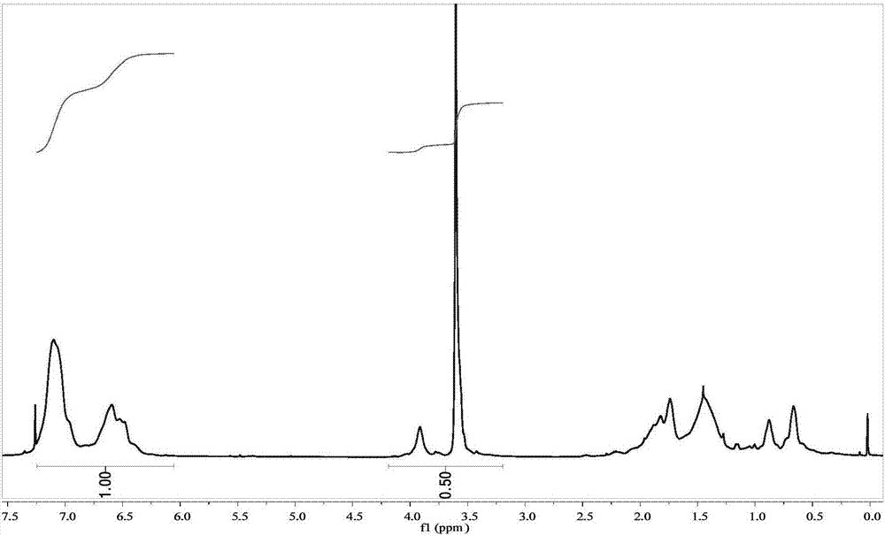
[0144] figure 1 For the block copolymer PS-PPDFMA-3-21 1 H-NMR spectrum.
[0145] from figure 1 It can be seen that the characteristic H peaks of both block...
Embodiment 2A
[0151] Example 2A type block copolymer PS-PPDFMA-3-46 (R 1 =CH 3 ,R 2 =C 12 H 10 F 15 , R 3 = none) preparation
[0152] 2 mL of styrene and 30 mL of tetrahydrofuran were treated with dibutylmagnesium solution (1 M, n-hexane as the solvent) at 40° C. for 0.5 h and transferred to a reaction flask. The reaction flask was returned to room temperature, stirred evenly, and then placed in a cooling bath at -50°C for 15 minutes. Add 0.5 mL of sec-BuLi (1M, the solvent is n-hexane), and keep the reaction at -50 °C for 15 min. The temperature of the dried modified methacrylate monomer A (1.6 g) was lowered to -30°C, dropped into the reaction system containing styrene, and kept at -50°C for 30 min. The product was precipitated in ethanol to give a white solid 2.6 g in 90% yield.
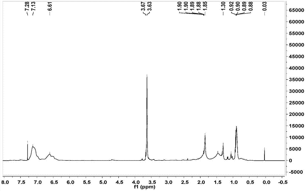
[0153] Block copolymer PS-PPDFMA-3-46 1 H-NMR spectrum and figure 1 similar.
[0154] The GPC results of the block copolymer PS-PPDFMA-3-46 were similar to those of PS-PPDFMA-3-21, with a number av...
PUM
| Property | Measurement | Unit |
|---|---|---|
| glass transition temperature | aaaaa | aaaaa |
| glass transition temperature | aaaaa | aaaaa |
| glass transition temperature | aaaaa | aaaaa |
Abstract
Description
Claims
Application Information