Battery piece PECVD post-plating film reworking piece processing method

A processing method and cell technology, applied in circuits, electrical components, sustainable manufacturing/processing, etc., can solve the problems of increasing the fragmentation rate of silicon wafers, increasing production costs, wasting acid materials, etc., and reducing the fragmentation rate of cell chips. , the effect of reducing the amount of use and reducing the concentration of use

Active Publication Date: 2017-11-07
TONGWEI SOLAR (ANHUI) CO LTD
View PDF5 Cites 8 Cited by
  • Summary
  • Abstract
  • Description
  • Claims
  • Application Information

AI Technical Summary

Problems solved by technology
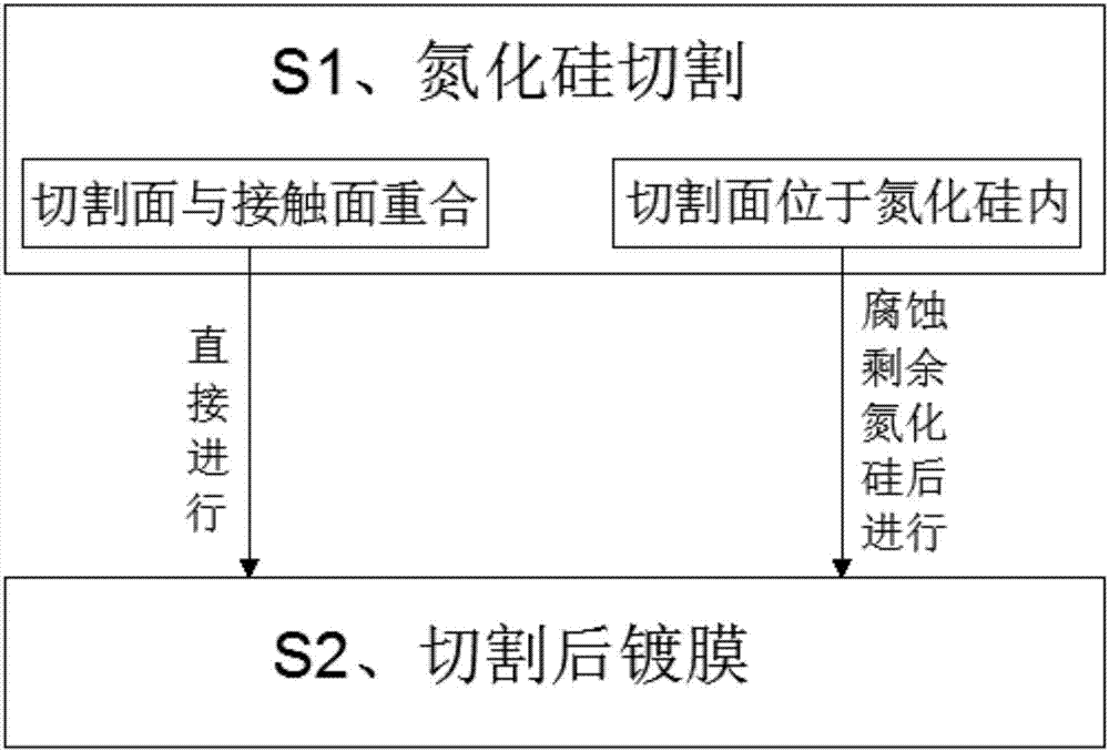
[0005] However, there are still obvious defects in the rework treatment methods of the above two patents for the color difference film: in the process of using HF acid solution to process the color difference film, the thickness of normal silicon nitride is 3-5 μm, and a large amount of silicon nitride is required to completely remove it with HF solution. The high concentration of HF acid is a waste of acid material
[0006] Chromatic aberration films need to go through high-concentration pickling to remove the silicon nitride and PN junction on the surface of the silicon wafer. The thickness of the removed silicon wafer is about 5 μm, and the texture is re-textured. The depth of the texture is 2-4 μm, and the diffusion process is 800 ° Reacting at the above temperature will cause damage to the silicon wafer, thereby increasing the fragmentation rate of the silicon wafer, increasing consumption, and increasing production costs.

Method used


Image

  • Battery piece PECVD post-plating film reworking piece processing method
  • Battery piece PECVD post-plating film reworking piece processing method
  • Battery piece PECVD post-plating film reworking piece processing method

Examples


Embodiment 1

[0026] A method for processing a reworked battery sheet after PECVD coating, comprising the following steps:

[0027] S1. Silicon nitride cutting: use a glass knife to cut and remove the silicon nitride on the surface of the cell;

[0028] First of all, place the color difference rework sheet in a clean environment to avoid pollution to the cell. Since the thickness of the cell is in microns, it is difficult to distinguish with the naked eye, so the silicon wafer can be operated under a microscope.

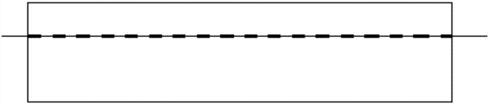
[0029] As attached to the manual figure 2 As shown, the thick dotted line in the figure is the contact surface between the cell and the deposited silicon nitride, and then the glass knife is controlled to align the contact surface. The cutting surface of the glass knife should always be kept parallel to the contact surface. In this embodiment, the cutting surface and the contact surface Overlapping, the thin solid line in the figure is the cutting surface line. After overlapping...

Embodiment 2

[0034] A method for processing a reworked battery sheet after PECVD coating, comprising the following steps:

[0035] S1. Silicon nitride cutting: use a glass knife to cut and remove the silicon nitride on the surface of the cell;

[0036] First of all, place the color difference rework sheet in a clean environment to avoid pollution to the cell. Since the thickness of the cell is in microns, it is difficult to distinguish with the naked eye, so the silicon wafer can be operated under a microscope.

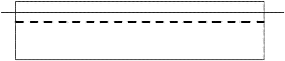
[0037] As attached to the manual image 3 As shown, the thick dotted line in the figure is still the contact surface between the cell and the deposited silicon nitride, and then the glass knife is controlled to align the silicon nitride. The cutting surface of the glass knife should always be kept parallel to the contact surface. In this embodiment, the cutting surface is located In the silicon nitride, the thin solid line in the figure is the cutting surface line, the glass knif...


PUM


Abstract

The invention discloses a battery piece PECVD post-plating film reworking piece processing method comprising the following steps: S1, silicon nitride cutting: using a glass knife to cut and remove the silicon nitride on the surface of the battery piece, specifically, if the glass knife cutting surface is located on the contact surface between the battery piece and the silicon nitride, directly entering step 2; S2, cutting and plating film: using a pipe type PECVD plating film process to re-plate films on the surface of the battery piece. The method can well remove the silicon nitride without using a HF acid solution or by using a little HF acid solution, and the texturization and PN node production cannot be affected; the method re-plate the PECVD film on the battery piece, thus effectively reducing battery piece damages and battery piece fragment rate, reducing raw material acid solution consumption, reducing production cost, improving work efficiency, and well processing aberration reworking pieces; the method is very effective.

Description

technical field [0001] The invention relates to the technical field of solar cell manufacturing, in particular to a method for processing reworked cells after PECVD coating. Background technique [0002] Solar cells mainly convert sunlight into electrical energy, which is a kind of green energy in real life. Solar cells are made of raw silicon wafers after cleaning the surface of silicon wafers, making texture, diffusing to form PN junctions, removing phospho-silicon glass, and depositing nitrogen. Formed by siliconization, printing, and sintering. [0003] Because most of the deposition of silicon nitride uses tubular PECVD (plasma enhanced chemical vapor deposition method), tubular PECVD has a certain influence on the uniformity of film thickness. The thickness of silicon nitride deposited on silicon wafers is different, and the present Different colors often cause chromatic aberration film. In the prior art, after the chromatic aberration film appears, it needs to be dri...

Claims


Application Information

Patent Timeline
Patent Type & Authority Applications(China)
IPC IPC(8): H01L31/18
CPCH01L31/186Y02P70/50
Inventor 刘文国苏世杰李强强张玉前尹丙伟
Owner TONGWEI SOLAR (ANHUI) CO LTD
Why Eureka
Try Eureka