Manufacturing method for improving uniwafer output of light emitting diode

A technology of light-emitting diodes and manufacturing methods, which is applied in semiconductor/solid-state device manufacturing, electrical components, circuits, etc., can solve the problems of reducing single-chip output, long production cycle, and high equipment cost, and achieve positive collapse and leakage improvement. Low cost, improve the effect of single chip output

Inactive Publication Date: 2017-11-24
YANGZHOU CHANGELIGHT
View PDF6 Cites 6 Cited by
  • Summary
  • Abstract
  • Description
  • Claims
  • Application Information

AI Technical Summary

Problems solved by technology

Although this method only needs to cut the chip twice to separate the core particles without contacting the PN junction surface, avoiding hard damage to the PN junction, but this process is easily affected by the isotropy of wet etching, and the distance between the core particles The loss width is

Method used


Image

  • Manufacturing method for improving uniwafer output of light emitting diode
  • Manufacturing method for improving uniwafer output of light emitting diode
  • Manufacturing method for improving uniwafer output of light emitting diode

Examples


Embodiment 1

[0041] 1) The distributed Bragg reflection layer, the N-type confinement layer, the active layer, the P-type confinement layer, and the window layer are epitaxially formed sequentially on the GaAs substrate.

[0042] 2) Use a new chromium plate with the same product name as the photolithographic plate with a core size 5 μm smaller than that of the conventional production process to make core grains and P electrode patterns on the window layer.

[0043] 3) An N electrode is formed on the bottom surface of the substrate to form an LED chip.

[0044] 4) Use a diamond blade with a thickness of 5 μm to half-cut the front of the LED chip. The knife speed is 10 mm / s, and the depth of the formed front cutting line is 10 μm, and the width is 5.2 μm. Each chip is cut. Pure water is used as cooling water during cutting, the temperature is 15°C, and the temperature fluctuation range does not exceed ±1°C.

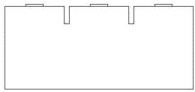
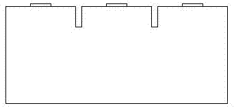
[0045] The results obtained are as image 3 shown.

[0046] 5) Unload the film and...

Embodiment 2

[0060] 1) A distributed Bragg reflection layer, an N-type confinement layer, an active layer, a P-type confinement layer, and a window layer are sequentially formed on the GaP substrate.

[0061] 2) Using a new chromium plate with the same product name as the conventional production process, the core grain size of the photolithography plate is 10 μm smaller, and the core grain and P electrode pattern are made on the window layer.

[0062] 3) An N electrode is formed on the bottom surface of the substrate to form an LED chip.

[0063] 4) Use ICP dry etching to photocut a dicing line on the front of the LED chip to obtain a front dicing line with a width of 20.3 μm and a depth of 50 μm.

[0064] The results obtained are as image 3 shown.

[0065] 5) Unload the film and test the photoelectric parameters.

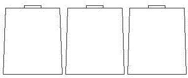
[0066] 6) Use a lithography machine with upper and lower CCD lenses to photocut a 30 μm wide and back-cutting aisle on the back of the LED chip corresponding to the front-s...

Embodiment 3

[0078] 1) A distributed Bragg reflection layer, an N-type confinement layer, an active layer, a P-type confinement layer, and a window layer are sequentially formed on the GaP substrate.

[0079] 2) Using a new chromium plate with the same product name as the conventional production process, the core grain size of the photolithography plate is 20 μm smaller, and the core grain and P electrode pattern are made on the window layer.

[0080] 3) An N electrode is formed on the bottom surface of the substrate to form an LED chip.

[0081] 4) Use a laser cutting machine to half-cut the front side of the LED chip, forming a front side cut line with a depth of 80 μm and a width of 30.1 μm.

[0082] The results obtained are as image 3 shown.

[0083] 5) Unload the film and test the photoelectric parameters.

[0084] 6) Using a photolithography machine with upper and lower CCD lenses, photocut a backside cutting track with a width of 60 μm on the back of the LED chip corresponding t...


PUM

PropertyMeasurementUnit
Depthaaaaaaaaaa
Thicknessaaaaaaaaaa
Thicknessaaaaaaaaaa

Abstract

The present invention provides a manufacturing method for improving uniwafer output of a light emitting diode, and relates to the production technology field of a quaternary system light emitting diode. A relatively thin blade is used at a right side for half cutting, or the ICP dry method etching and laser cutting is employed to make cutting channels with a certain width and depth, a cutting walk way is subjected to photoetching at a back side, the dry method etching technology is employed to etch a cutting channel with a certain depth, and a relative thick blade is used to cut through a LED chip at the back side. The production efficiency is improved, the positive collapse is reduced, a chip gain structure with a big the right side and a small back side is obtained, the absorption of the substrate for light is reduced, the emergent light from the right side is increased, and the light extraction efficiency is increased.

Description

technical field [0001] The invention relates to the technical field of production of quaternary light-emitting diodes. Background technique [0002] Light-emitting diodes (LED for short) can be divided into red, yellow, blue, green, etc. according to their colors. Use MOCVD epitaxial furnace to grow InGaN, GaN and other structures on silicon carbide and sapphire substrates to obtain blue and green high-brightness light-emitting diodes; grow AlGaInP materials on GaAs substrates to obtain color coverage from red, orange, yellow, to Light-emitting diodes in the yellow-green band. Compared with incandescent bulbs and xenon lamps, it has the advantages of low operating voltage and current, high reliability, long life and convenient adjustment of luminous brightness. Widely used in backlight, landscape decorative lighting, traffic lights, indoor and outdoor display screens, automobile tail lights and lighting and other fields. [0003] Usually, the red, orange, yellow, and yell...

Claims


Application Information

Patent Timeline
IPC IPC(8): H01L33/00H01L21/304
CPCH01L33/0062H01L21/304
Inventor 何胜李俊承杨凯张双翔陈凯轩
Owner YANGZHOU CHANGELIGHT
Why Eureka
Try Eureka