
LED epitaxial growth method
An epitaxial growth and epitaxy technology, applied in the direction of crystal growth, single crystal growth, single crystal growth, etc., can solve the problems of increasing the number of electron-hole pairs in the multi-quantum well layer, affecting the luminous efficiency of LEDs, and improving the level of hole injection. , the effect of increasing the number and reducing the working voltage
Patent Information
- Authority / Receiving Office
- CN · China
- Current Assignee / Owner
- Publication Date
- 2017-11-24
Smart Images
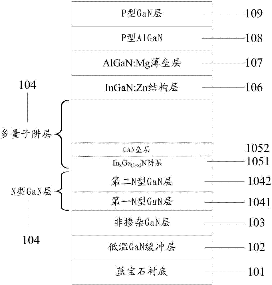
Figure 1 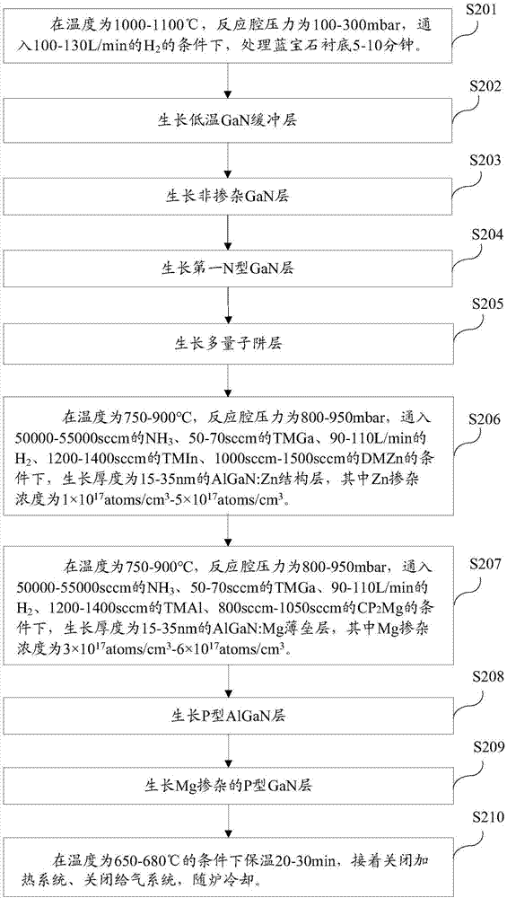
Figure 2 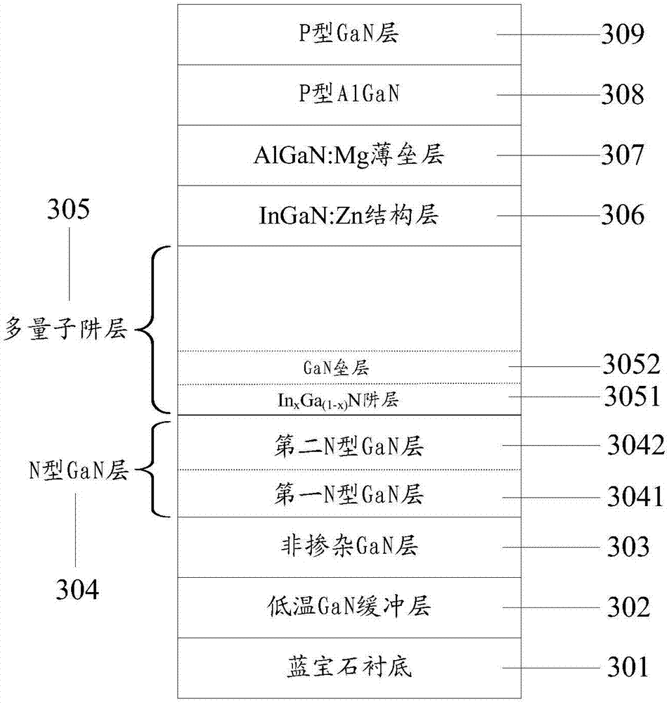
Figure 3
Abstract
Description
technical field
[0001] The invention belongs to the technical field of LEDs, and in particular relates to an LED epitaxial growth method. Background technique
[0002] A light-emitting diode (Light-Emitting Diode, LED) is a semiconductor electronic device that converts electrical energy into light energy. When electric current flows, electrons and holes recombine in it to emit monochromatic light. As a high-efficiency, environmentally friendly, and green new solid-state lighting source, LED has the advantages of low voltage, low power consumption, small size, light weight, long life, high reliability, and rich colors. At present, the scale of domestic production of LEDs is gradually expanding, but LEDs still have the problem of low efficiency.
[0003] The traditional LED structure epitaxial growth method includes the following steps:
[0004] 1. At a temperature of 1000-1100°C and a reaction chamber pressure of 100-300mbar, feed 100-130L / min of H 2 Under certain conditi...
Examples
Embodiment 1
[0053] This embodiment provides an LED epitaxial growth method, figure 1 A schematic structural diagram of the LED epitaxy prepared by the LED epitaxy growth method in this embodiment is given, please refer to figure 1 , the LED epitaxy, including: a low-temperature GaN buffer layer 102, a non-doped GaN layer 103, an N-type GaN layer 104, a multi-quantum well layer 105, an InGaN:Zn structure layer 106, an AlGaN: Mg thin barrier layer 107 , P-type AlGaN layer 108 and P-type GaN layer 109 . Wherein, the N-type GaN layer 104 includes a first N-type GaN layer 1041 and a second N-type GaN layer 1042; the multi-quantum well layer 105 includes alternately grown In x Ga (1-x) The alternating period of the N well layer 1051 and the GaN barrier layer 1052 is controlled at 7-15.
[0054] The LED epitaxial growth method provided in this embodiment uses MOCVD to grow high-brightness GaN-based LED epitaxial wafers, and uses high-purity H 2 or high purity N 2 or high purity H 2 and hig...
Embodiment 2
[0067] This embodiment provides an LED epitaxial growth method, image 3 A schematic structural diagram of the LED epitaxy prepared by the LED epitaxy growth method in this embodiment is given, please refer to image 3 , the LED epitaxy, including: a low-temperature GaN buffer layer 302, a non-doped GaN layer 303, an N-type GaN layer 304, a multi-quantum well layer 305, an InGaN:Zn structure layer 306, an AlGaN: Mg thin barrier layer 307 , P-type AlGaN layer 308 and P-type GaN layer 309 . Wherein, the N-type GaN layer 104 includes a first N-type GaN layer 1041 and a second N-type GaN layer 1042; the multi-quantum well layer 305 includes alternately grown In x Ga (1-x) The alternating period of the N well layer 3051 and the GaN barrier layer 3052 is controlled at 7-15.
[0068] The LED epitaxial growth method provided in this embodiment uses MOCVD to grow high-brightness GaN-based LED epitaxial wafers, and uses high-purity H 2 or high purity N 2 or high purity H 2 and hig...