Eureka AIR delivers breakthrough ideas for toughest innovation challenges, trusted by R&D personnel around the world.

Processing method for ladder pore arrays with extremely-small pore diameters

A processing method and stepped hole technology, which is applied in the formation of specific nanostructures, nanostructure manufacturing, nanotechnology, etc., can solve the complex process of the silicon secondary filling and inversion method, the difficulty in meeting high-performance detection, and the difficulty in processing micropore groups, etc. low cost, easy operation and good compatibility

Active Publication Date: 2017-12-22
广东省先进陶瓷材料科技有限公司
View PDF8 Cites 0 Cited by
  • Summary
  • Abstract
  • Description
  • Claims
  • Application Information

AI Technical Summary

Problems solved by technology

[0003] At present, the methods for processing nanohole arrays with small apertures mainly include photolithography, electrochemical etching, reactive ion etching (RIE), and silicon secondary filling inversion method, among which reactive ion etching (RIE) is not suitable. It is used to process nanopore arrays with high specific surface area; the silicon secondary filling and inversion method is complex in process, high in cost, and difficult in industrialization
The in-situ photo-synthesis technology combined with solid-phase chemistry and photolithography technology is limited by the resolution of the photolithography machine (currently the highest resolution is 10nm), and it is difficult to process micropore groups with a pore diameter of only 5nm. Existing methods The pore diameter of the processed microhole array is generally 20-100nm, and the shape of the microhole array is usually a straight hole, which is difficult to meet the requirements of high-performance detection

Method used


Image

  • Processing method for ladder pore arrays with extremely-small pore diameters
  • Processing method for ladder pore arrays with extremely-small pore diameters
  • Processing method for ladder pore arrays with extremely-small pore diameters

Examples


Embodiment 2

[0082] The method for processing a three-level stepped hole array in this embodiment includes the following steps:

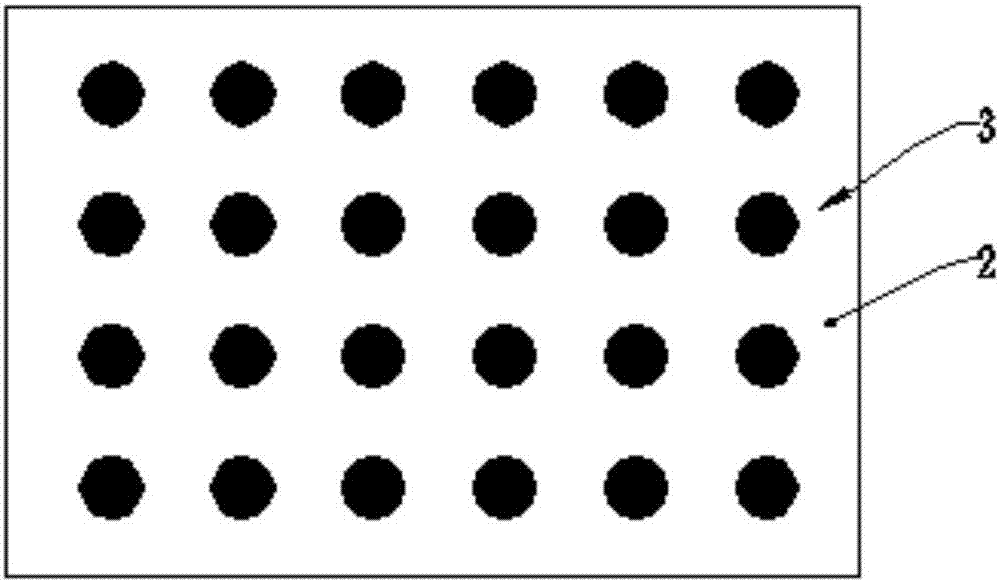
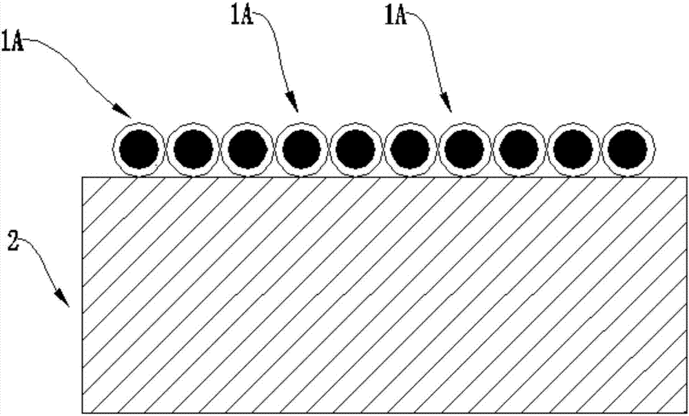
[0083] Step 1: First, select a silicon wafer with a size of 25mm×25mm×0.5mm (length*width*thickness) as the workpiece 2, and put the workpiece 2 into ethanol and deionized water for 30 minutes for ultrasonic cleaning respectively, and then wash the concentrated sulfuric acid Heat the mixed solution with hydrogen peroxide to 120°C, put the ultrasonically cleaned workpiece 2 into it and soak for 20 minutes, rinse repeatedly to remove the acidic substances after soaking, and then put the workpiece 2 into a 60°C cleaning solution made of ammonia, hydrogen peroxide and water. Soak in the solution for 20 minutes, take it out, rinse it repeatedly with deionized water, and then dry it with nitrogen to remove oxides on the surface of the workpiece 2, and finally obtain a clean workpiece 2 with good hydrophilicity.

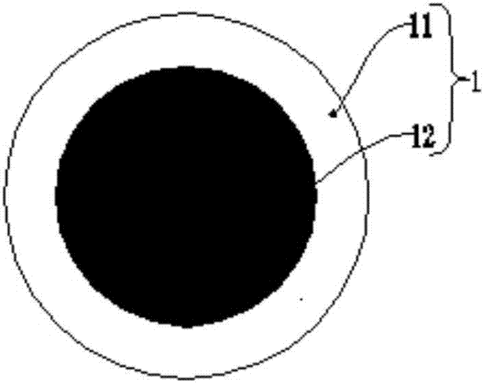
[0084] Step 2: prepare the first-grade core-shell nanos...


PUM

PropertyMeasurementUnit
particle diameteraaaaaaaaaa

Abstract

The invention discloses a processing method for ladder pore arrays with extremely-small pore diameters. According to the ladder pore arrays required shaping, core-shell nano balls which are formed by a noble metal wrapped with silicon dioxide (SiO2) are selected and used as machining tools, separately through thickness of a silicon dioxide layer which is located at an outer layer of each core-shell nano ball and particle sizes of noble metal particles, spacing and pore sizes of ladder pores are controlled, in an etching solution, workpieces are processed to obtain high-density microporous arrays, and through a multi-step method, different-size noble metal particles are further selected and used, so that the ladder pore arrays of which required pore diameters are gradually decreased are obtained. The method is simple in a process, required raw materials such as the core-shell nano balls with relatively-good monodispersity, and the silicon dioxide nano balls are mature, the method can control the diameters of the raw materials to be 5nm or less, and provides support for processing microporous arrays of which pore diameters are less than 5nm.

Description

technical field [0001] The invention relates to the field of nano-device processing, in particular to a processing method for a stepped hole array with extremely small apertures. Background technique [0002] Microwell arrays are widely used in microfluidic chips, biochips and microelectronic devices, and are often used in various important applications such as controlling various types of chemical reactions, screening abnormal cells, genetic testing, and electrical channels. The density, pore size, and structure of the microwell array directly affect the accuracy of control and detection. Especially in high-end applications such as genetic testing, the pore diameter is required to be less than 10nm, and the shape is a stepped hole. [0003] At present, the methods for processing nanohole arrays with small apertures mainly include photolithography, electrochemical etching, reactive ion etching (RIE), and silicon secondary filling inversion method, among which reactive ion e...

Claims


Application Information

Patent Timeline
Patent Type & Authority Applications(China)
IPC IPC(8): B82B3/00B82Y40/00
CPCB82B3/0009B82Y40/00
Inventor 陈云陈新麦锡全刘强高健高波
Owner 广东省先进陶瓷材料科技有限公司
Why Eureka
Eureka Blog
Learn More