Film manufacturing method

A thin film and sputtering technology, applied in ion implantation plating, metal material coating process, coating and other directions, can solve the problems of high demand, low deposition rate, small sputtering energy, etc., to prolong the process time, reduce Deposition rates, results for demanding needs

Active Publication Date: 2017-12-26
BEIJING NAURA MICROELECTRONICS EQUIP CO LTD
View PDF4 Cites 7 Cited by
  • Summary
  • Abstract
  • Description
  • Claims
  • Application Information

AI Technical Summary

Problems solved by technology

In the sputtering process, to obtain a high-density film requires greater sputtering energy, faster deposition rate, higher process temperature, lower sputtering process pressure, etc. However, to obtain a film with greater stress Higher process pressure

Method used


Image

  • Film manufacturing method
  • Film manufacturing method
  • Film manufacturing method

Examples


Embodiment 1

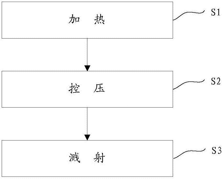
[0041] The film forming method is used to form a thin film by sputtering on a wafer, the wafer is located on a base, the base is placed at the bottom of a reaction chamber, and a target is arranged on the top of the reaction chamber.

[0042] As an embodiment, a specific film-making method includes the following steps:

[0043]S11) Heating step: feeding the first gas into the reaction chamber, and controlling the flow of the first gas, so that the first air pressure in the reaction chamber remains constant; at the same time, heating the wafer to a set temperature.

[0044] Preferably, the first gas is argon, the first pressure is 1T-2T; the heating temperature is 300° C.-400° C., and the heating time is 1 min.

[0045] In this step, the wafer is introduced into the reaction chamber, Ar is introduced into the reaction chamber, the air pressure reaches 1T-2T, the susceptor temperature is set at 300°C-400°C, wait for about 1min, and the susceptor is aligned with the wafer. circl...

Embodiment 2

[0055] The film forming method is used to form a thin film by sputtering on a wafer, the wafer is located on a base, the base is placed at the bottom of a reaction chamber, and a target is arranged on the top of the reaction chamber.

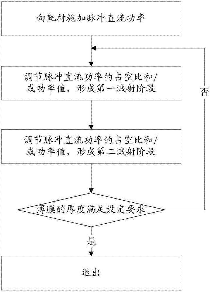
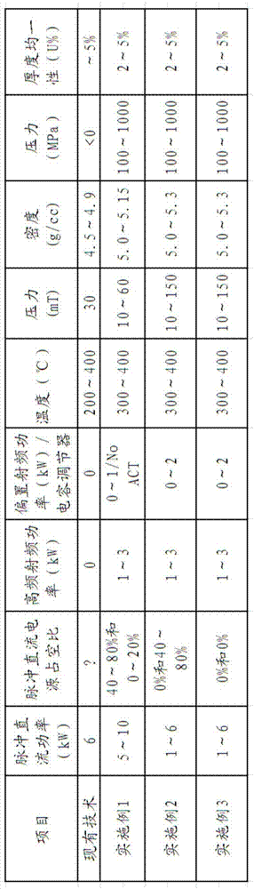
[0056] Compared with the previous embodiment, the film forming method in this embodiment differs in that: on the basis of pulsed DC power, RF power is further applied to the target, and RF power is applied to the target to start the ignition. The high-frequency radio frequency power is still maintained in the sputtering stage, and the high-frequency radio frequency power is turned off in the second sputtering stage.

[0057] As an embodiment, a specific film-making method includes the following steps:

[0058] S21) Heating step: feeding the first gas into the reaction chamber, and controlling the flow of the first gas, so that the first air pressure in the reaction chamber remains constant; at the same time, heating the wafer to a set temperatur...

Embodiment 3

[0073] The film forming method is used to form a thin film by sputtering on a wafer, the wafer is located on a base, the base is placed at the bottom of a reaction chamber, and a target is arranged on the top of the reaction chamber.

[0074] Compared with the previous embodiment, the film forming method in this embodiment differs in that: on the basis of pulsed DC power, RF power is further applied to the target, and RF power is applied to the target to start the ignition. Both the sputtering stage and the second sputtering stage maintain high frequency RF power.

[0075] As an embodiment, a specific film-making method includes the following steps:

[0076] S31) Heating step: feeding the first gas into the reaction chamber, and controlling the flow of the first gas so that the first air pressure in the reaction chamber remains constant; at the same time, heating the wafer to a set temperature.

[0077] Preferably, the first gas is argon, the first pressure is 1T-2T; the heat...


PUM

PropertyMeasurementUnit
Densityaaaaaaaaaa
Stressaaaaaaaaaa

Abstract

The invention belongs to the technical field of semiconductor processing and particularly relates to a film manufacturing method. The film manufacturing method is used for forming a thin film on a wafer in a sputtering mode and comprises a sputtering step. The sputtering step comprises a first sputtering stage and a second sputtering stage which are circularly conducted, and thus the density and stress of the thin film are adjusted till the thickness of the thin film meets the setting requirement. According to the film manufacturing method, the mode that a pulsed direct current is applied to a target material in a sputtering mode is adopted, the duty ratio and/or the power value of the pulsed direct current power are/is adjusted to control the deposition speed rate of the thin film, the situation that under the high power, sputtering energy is increased without increasing the deposition speed rate of the thin film is achieved, the relation between the deposition speed rate and the sputtering energy is balanced, the compactness of the thin film is improved, the deposition speed rate of thin film is properly decreased, the process time of the thin film is prolonged, the production stability is improved, and the thin film with larger stress is obtained.

Description

technical field [0001] The invention belongs to the technical field of semiconductor processing, and in particular relates to a film forming method. Background technique [0002] In recent years, with the large-scale development of integrated circuits, the critical dimensions of chips have been continuously reduced, and the manufacturing process of copper interconnection is facing more and more challenges. In order to ensure the compactness and structural integrity of the copper interconnect structure below 16nm and smaller, more advanced hard mask technology is required. In a more advanced process manufacturing process, the main function of hard mask technology (Hardmask) is to maintain the pattern integrity of copper lines and vias in softer ultra-low-k dielectric materials. However, with the continuous shrinking of the chip manufacturing process size, there are many problems in the traditional hard mask layer (such as TiN layer), which cannot be applied to more advanced ...

Claims


Application Information

Patent Timeline
IPC IPC(8): C23C14/34
CPCC23C14/3485
Inventor 耿波白志民王厚工丁培军赵晋荣罗建恒张超
Owner BEIJING NAURA MICROELECTRONICS EQUIP CO LTD
Why Eureka
Try Eureka