Semiconductor device and forming method thereof

A semiconductor and device technology, applied in the field of semiconductor devices and their formation, can solve the problem that the electrical performance of the device needs to be improved, etc.

Active Publication Date: 2018-01-16
SEMICON MFG INT (SHANGHAI) CORP +1
View PDF5 Cites 4 Cited by
  • Summary
  • Abstract
  • Description
  • Claims
  • Application Information

AI Technical Summary

Problems solved by technology

[0004] Although the introduction of a high-k metal gate can improve the electrical performance of the device to a certain extent, the electrical performance of the device formed by the prior art still needs to be improved.

Method used


Image

  • Semiconductor device and forming method thereof
  • Semiconductor device and forming method thereof
  • Semiconductor device and forming method thereof

Examples


Embodiment Construction

[0019] According to the background art, the electrical performance of semiconductor devices formed in the prior art needs to be improved.

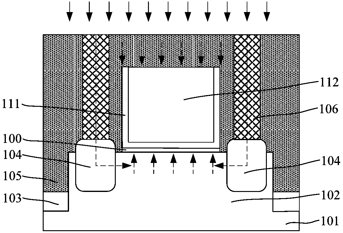
[0020] refer to figure 1 , figure 1 It is a schematic cross-sectional structure diagram of a semiconductor device, which includes: a substrate 101, a fin 102 located on the substrate 101; an isolation layer 103 located on the substrate 101 and covering part of the sidewall of the fin 102; The gate structure of the fin 102, the gate structure covers the top and side walls of the fin, wherein the gate structure at least includes a high-k gate dielectric layer 111, a high-k gate dielectric layer 111 The gate electrode layer 112; the source-drain doped region 104 in the fin portion 102 located on both sides of the gate structure; the dielectric layer 105 located on the isolation layer 103 and the fin portion 102, and the dielectric layer 105 also covers the gate The top and side walls of the electrode structure; the conductive plug 106 locat...


PUM


Abstract

The invention discloses a semiconductor device and a forming method thereof. The forming method comprises steps: a first conductive plug is formed inside an interlayer dielectric layer, wherein the first conductive plug is electrically connected with a source and drain doping area; before or after the first conductive plug is formed, a gate electrode layer with a first thickness is etched and removed, and a blocking layer is formed at the top part of the gate electrode layer after etching; an upper dielectric layer is formed on the interlayer dielectric layer and the blocking layer; a second conductive plug passing through the upper dielectric layer is formed in the upper dielectric layer; and annealing treatment is carried out, the annealing treatment is carried out in an atmosphere containing passivated ions, the passivated ions are diffused to the base below the gate structure through the second conductive plug and the first conductive plug, and the passivated ions located in the base are diffused to a gate dielectric layer. While the interface performance between the gate structure and the base is improved, the passivated ions can be prevented from being diffused inside the gate electrode layer, and the electrical performance of the formed semiconductor device is thus improved.

Description

technical field [0001] The invention relates to the technical field of semiconductors, in particular to a semiconductor device and a forming method thereof. Background technique [0002] The main semiconductor device of an integrated circuit, especially a very large scale integrated circuit, is a metal-oxide-semiconductor field effect transistor (MOS transistor). With the continuous development of integrated circuit manufacturing technology, the technology nodes of semiconductor devices are continuously reduced, and the geometric dimensions of semiconductor structures are continuously reduced following Moore's law. When the size of the semiconductor structure is reduced to a certain extent, various secondary effects caused by the physical limit of the semiconductor structure appear one after another, and it becomes more and more difficult to scale down the feature size of the semiconductor structure. Among them, in the field of semiconductor manufacturing, the most challeng...

Claims


Application Information

Patent Timeline
Patent Type & Authority Applications(China)
IPC IPC(8): H01L21/8238H01L21/28H01L21/768H01L27/092H01L29/423
Inventor 李勇
Owner SEMICON MFG INT (SHANGHAI) CORP
Why Eureka
Try Eureka