Wide-spectrum response photodetector and preparation method thereof

A photodetector and broad-spectrum technology, applied in the field of wide-spectrum response photodetectors and their preparation, can solve the problems of narrow spectral response range and weak light absorption ability, achieve high responsivity and detection rate, and improve device reliability , the effect of low dark current density

Active Publication Date: 2019-09-03
XIDIAN UNIV
View PDF3 Cites 2 Cited by
  • Summary
  • Abstract
  • Description
  • Claims
  • Application Information

AI Technical Summary

Problems solved by technology

[0004] The current photodetectors have problems such as weak light absorption ability and narrow spectral response range.

Method used


Image

  • Wide-spectrum response photodetector and preparation method thereof
  • Wide-spectrum response photodetector and preparation method thereof
  • Wide-spectrum response photodetector and preparation method thereof

Examples


Embodiment 1

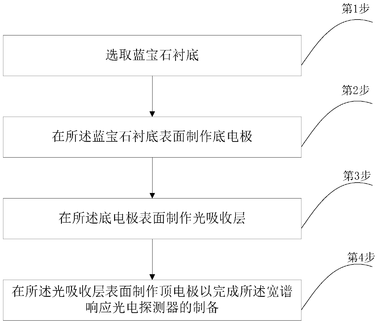
[0042] See figure 1 , figure 1 A flow chart of a preparation method of a photodetector with a broad-spectrum response provided by an embodiment of the present invention, wherein the preparation method includes:

[0043] (a) select a sapphire substrate;

[0044] (b) making a bottom electrode on the surface of the sapphire substrate;

[0045] (c) making a light absorbing layer on the surface of the bottom electrode;

[0046] (d) Fabricating a top electrode on the surface of the light-absorbing layer to complete the preparation of the broad-spectrum response photodetector.

[0047] Preferably, step (b) may include:

[0048] (b1) using a magnetron sputtering process to grow a first metal material on the surface of the sapphire substrate;

[0049] (b2) Forming an ohmic contact between the sapphire substrate and the first metal material by using a rapid thermal annealing process in an atmosphere of nitrogen and argon to complete the preparation of the bottom electrode.

[0050...

Embodiment 2

[0075] Please refer to Figure 2a-Figure 2f , Figure 2a-Figure 2f It is a schematic diagram of a preparation method of a wide-spectrum response photodetector according to an embodiment of the present invention, and the preparation method includes the following steps:

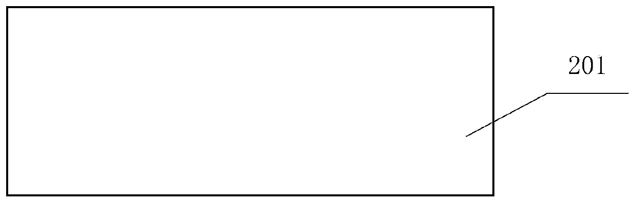
[0076] Step 1, select sapphire substrate 201, such as Figure 2a shown.

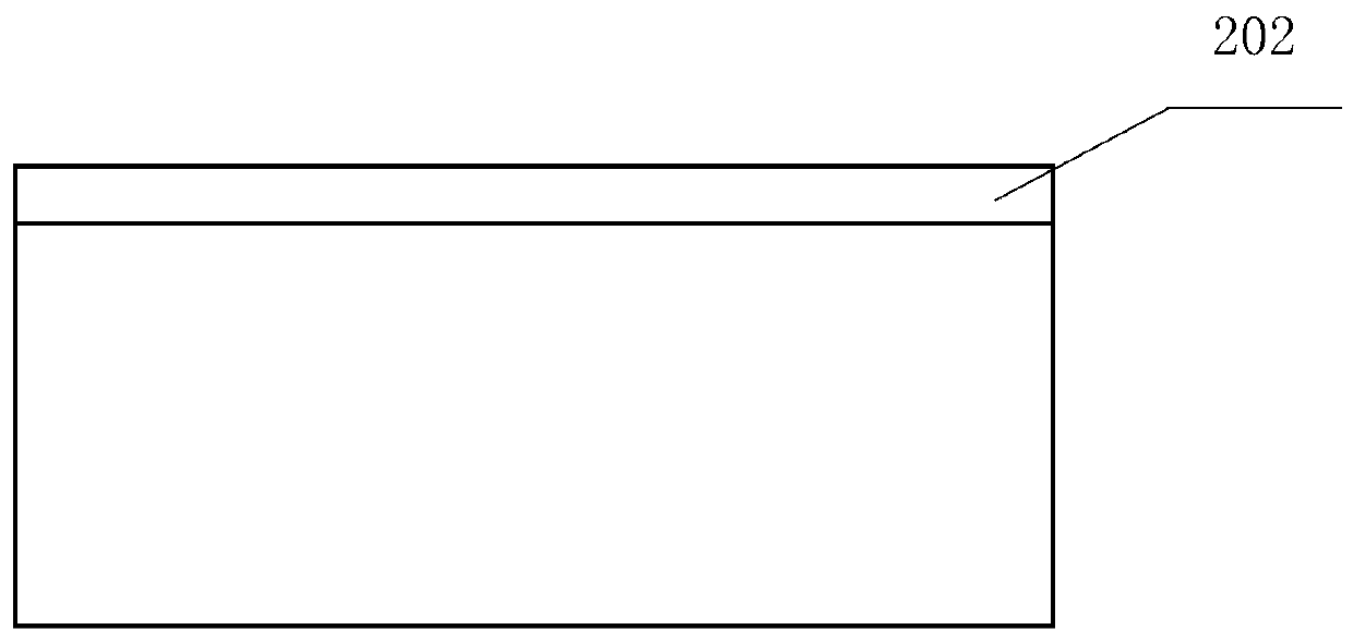
[0077] Step 2: Sputter Ti material on the surface of sapphire substrate 201 by using magnetron sputtering process; under the atmosphere of nitrogen and argon, utilize rapid thermal annealing process to form ohmic contact between sapphire substrate 201 and Ti material to complete The bottom electrode 202 is prepared as Figure 2b shown.

[0078] Step 3, using the magnetron sputtering process to grow Ga on the surface of the bottom electrode 202 2 o 3 , as the first light absorbing layer 203 such as Figure 2c shown.

[0079] Step 4, preparing a spin-coating precursor solution; spin-coating the precursor solution onto the surface of...

Embodiment 3

[0084] Please refer to image 3 , image 3 A schematic structural diagram of a wide-spectrum response photodetector provided by an embodiment of the present invention. The photodetector employs the above-mentioned as Figure 2a-Figure 2f prepared as indicated. Specifically, the photodetector includes: a sapphire substrate 301, a bottom electrode 302, a Ga 2 o 3 Light absorbing layer 303, hybrid perovskite light absorbing layer 304, β-Ga 2 o 3 The light absorbing layer 305 and the top electrode 306 .


PUM


Abstract

The invention relates to a wide spectrum response photoelectric detector and a preparation method thereof. The preparation method comprises the steps that (a) a sapphire substrate is selected; (b) a bottom electrode is manufactured on the surface of the sapphire substrate; (c) a light absorption layer is manufactured on the surface of the bottom electrode; and (d) a top electrode is manufactured on the surface of the light absorption layer so as to complete preparation of the wide spectrum response photoelectric detector. According to the wide spectrum response photoelectric detector, the double-heterojunction structure is adopted so that double potential barriers can be formed, the leakage current can be effectively reduced and the device reliability of the photoelectric detector can be greatly enhanced.

Description

technical field [0001] The invention relates to the field of semiconductor device design and manufacture, in particular to a wide-spectrum response photodetector and a preparation method thereof. Background technique [0002] At present, most photodetectors are photodetection diodes based on PN junctions, which can generally measure ultraviolet to infrared light regions, and have great use value in the development of military high-tech and civilian product markets, such as detecting tail smoke or Flying targets that can emit a large amount of ultraviolet radiation in the plume can be detected or effectively tracked in real time. In the infrared region, near-infrared detection plays an important role in resource investigation, environmental monitoring, medical diagnosis, night vision imaging and other fields. [0003] Based on CH 3 NH 3 PB 3 Perovskite materials are widely used in photodetectors, which have high response from visible light to near-infrared. However, these...

Claims


Application Information

Patent Timeline
Patent Type & Authority Patents(China)
IPC IPC(8): H01L51/42H01L51/46H01L51/48
CPCY02E10/549Y02P70/50
Inventor 贾仁需庞体强栾苏珍张玉明汪钰成刘银涛
Owner XIDIAN UNIV
Why Eureka
Try Eureka