Electronic control liquid crystal adjustable terahertz wave absorber based on synchronous drive of graphene/metamaterial and preparing method of electronic control liquid crystal adjustable terahertz wave absorber
A graphene and metamaterial technology, applied in the field of terahertz optoelectronics, can solve the problems that the metal layer cannot meet the requirements, it is difficult to achieve practicality, and the amount of controllability is small, so as to achieve good electric field distribution, the ability to control liquid crystal, and low absorption loss , The effect of stable device performance
- Summary
- Abstract
- Description
- Claims
- Application Information
AI Technical Summary
Problems solved by technology
Method used
Image
Examples
Embodiment 1
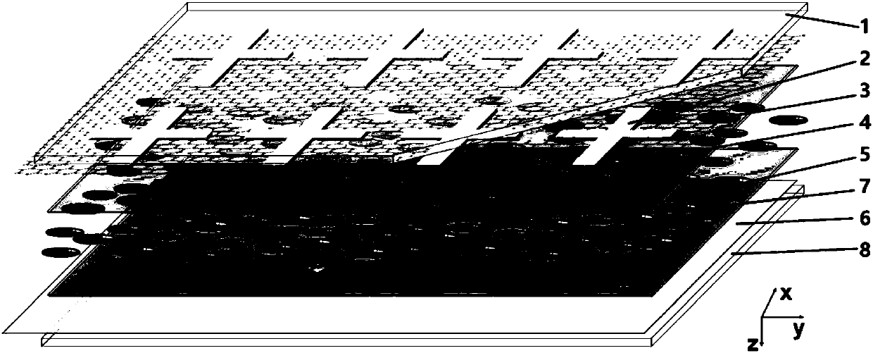
[0038] An electronically controlled liquid crystal tunable terahertz wave absorber based on graphene / metamaterial synergistic drive, refer to figure 1 , the absorber includes a quartz substrate a1, a liquid crystal layer 5 and a quartz substrate b8, the quartz substrate a1 and the quartz substrate b8 are combined by a sealant to form a liquid crystal cell, and the liquid crystal layer 5 is provided on the quartz substrate a1 and the quartz substrate b. 8 junctions.
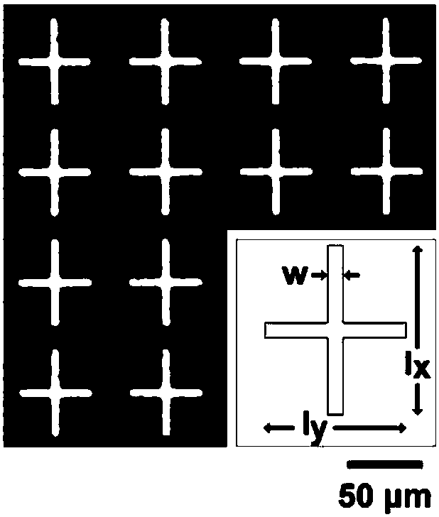
[0039]The inner side of the quartz substrate a 1 includes a periodic sub-wavelength metal element array 2, a porous graphene layer 3 and a light alignment layer a 4 in turn from inside to outside, and the periodic sub-wavelength metal element array 2 selects a cross-shaped metal element array, and the periodic The thickness is 150 μm, which is less than the wavelength of the incident light terahertz, and the thickness is 100 nm. The number of graphene layers in the porous graphene layer 3 is 3, and the surface of ...
Embodiment 2
[0051] This embodiment is a disc-type electronically controlled liquid crystal tunable terahertz wave absorber, and the specific structural design is as follows Figure 7 As shown, the structure is the same as that of the absorber described in Example 1, except that the periodic subwavelength metal element array 2 is disc-shaped, the diameter of the disc is 130 μm, the period is 150 μm, and the thickness of the liquid crystal layer is 10 μm.
[0052] The specific preparation process is as follows:
[0053] Step 1. Take the quartz substrate a 1 and the quartz substrate b 8 for melting, and set the disk-shaped periodic sub-wavelength metal element array 2 on the inner side of the fused silica substrate a 1 through photolithography and coating processes. The preparation method of array 2 is as follows: photolithography and development are carried out on the fused silica substrate a1, a photolithography template with a diameter of 130 μm is selected, and then a gold film with a th...
PUM
| Property | Measurement | Unit |
|---|---|---|
| thickness | aaaaa | aaaaa |
| thickness | aaaaa | aaaaa |
| thickness | aaaaa | aaaaa |
Abstract
Description
Claims
Application Information


