
Single-end-to-differential transimpedance amplifier based on CMOS process

A single-ended to differential, transimpedance amplifier technology, applied in the field of amplifiers, can solve the problems of optical receiver bit error rate and other performance degradation, limited output swing increase, gain limitation, etc., to improve power supply rejection ratio, increase gain, The effect of reducing the difficulty of design

Inactive Publication Date: 2018-03-02
TIANJIN UNIV
View PDF5 Cites 1 Cited by
  • Summary
  • Abstract
  • Description
  • Claims
  • Application Information

AI Technical Summary

Problems solved by technology

[0006] 2. Limitation of gain by low supply voltage
[0007] 3. Noise limit
In order to increase the transmission rate of the optical receiver, most of the current front-end transimpedance amplifier circuits of the optical receiver use a regulated cascode structure (RGC) instead of the traditional common source feedback structure. The RGC structure can reduce the input resistance and increase the transimpedance. The bandwidth of the amplifier, but compared with the transimpedance amplifier of the common source feedback structure, the larger noise introduced by the RGC structure reduces the performance of the optical receiver such as the bit error rate
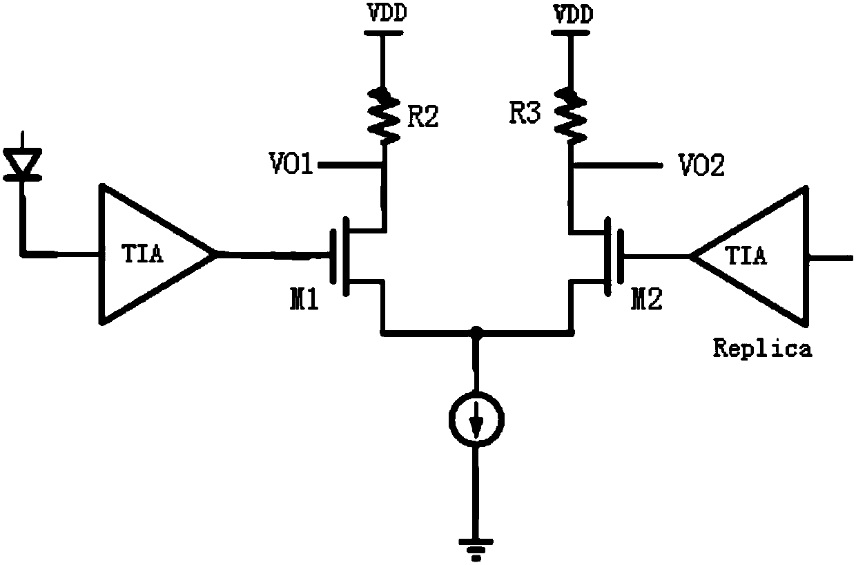
[0008] Generally speaking, the front-end transimpedance amplifiers of optical receivers based on CMOS technology mostly use single-ended or pseudo-differential structures. The signals provided by this structure for subsequent limiting amplifiers are single-ended or pseudo-differential signals. limits the output swing boost

Method used


Image

  • Single-end-to-differential transimpedance amplifier based on CMOS process
  • Single-end-to-differential transimpedance amplifier based on CMOS process
  • Single-end-to-differential transimpedance amplifier based on CMOS process

Examples


Embodiment Construction

[0023] A CMOS process-based single-ended-to-differential transimpedance amplifier of the present invention will be described in detail below in combination with embodiments and drawings.

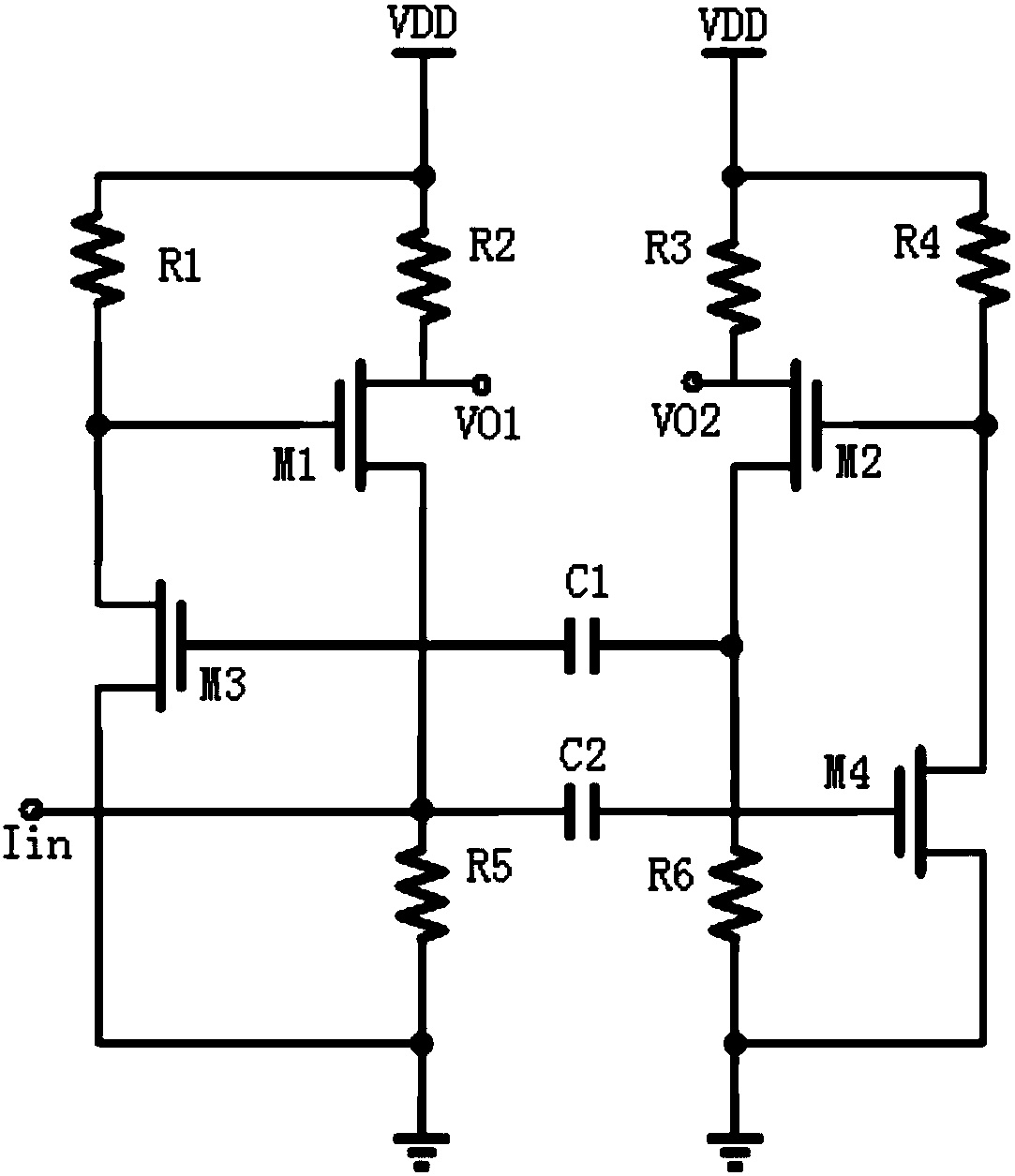
[0024] A single-ended to differential transimpedance amplifier based on CMOS technology of the present invention, by introducing transconductance enhancement technology and capacitive coupling technology into the optical receiver preamplifier circuit, a single-ended input differential output, low-noise transimpedance amplifier is designed. resistance amplifier. A coupling input circuit composed of source resistors and capacitors; a transconductance enhancement stage formed by a common source amplifier between the gate and the input terminal; a differential output stage formed by a differential pair, together constitute a single-slip transimpedance amplifier. Specifically, the capacitive coupling circuit formed by the capacitor and the source bias resistor divides the single-ended current sig...


PUM


Abstract

The invention provides a single-end-to-differential transimpedance amplifier based on CMOS process. The grid of a first MOS tube and the drain of a third MOS tube are connected with a power supply through first resistors, the grid of a second MOS tube and the drain of a fourth MOS tube are connected with the power supply through fourth resistors, the drains of the first MOS tube and the second MOStube are connected with the power supply through a second resistor and a third resistor, the source electrode of the first MOS tube is separately connected with one end of a second capacitor, one endof a fifth resistor and a single-end current input end, the source electrode of the second MOS tube is separately connected with one end of a first capacitor and one end of a sixth resistor, the other end of the second capacitor is connected with the grid of the fourth MOS tube, the other ends of the fifth resistor and the sixth resistor are grounded, the drains of the first MOS tube and the second MOS tube form a first output end and a second output end. The single-end-to-differential transimpedance amplifier improves the gain of the cross resistance amplifier and reduces the noise.

Description

technical field [0001] The present invention relates to an amplifier. In particular, it relates to a CMOS technology-based single-end-to-differential transimpedance amplifier applied to a single-end-to-differential optical receiver circuit. Background technique [0002] With the rapid development of informatization, concepts such as "cloud computing" and "big data" have gradually moved from theory to practical application fields, and play a vital role in the national economy and people's livelihood. The explosive data volume required by the wide application of cloud services puts forward high requirements on data transmission bandwidth. The traditional electrical interconnection data transmission mode has problems such as electromagnetic interference and large transmission loss in the high-speed data transmission mode, making it difficult to meet the needs of high-speed big data transmission in the context of informatization. The optical interconnection data transmission m...

Claims


Application Information

Patent Timeline
Patent Type & Authority Applications(China)
IPC IPC(8): H03F1/32H03F3/08H03F3/45
CPCH03F1/3211H03F3/082H03F3/45179H03F2200/294H03F2203/45032H03F2203/45151H03F2203/45156
Inventor 毛陆虹周高磊谢生
Owner TIANJIN UNIV
Learn More