Preparation method of graphene field effect transistor based on bubbling

A field-effect transistor, graphene technology, applied in transistors, semiconductor/solid-state device manufacturing, electric solid-state devices, etc., can solve problems such as difficult control, high cost, complex process, etc., to avoid damage to the channel, avoid pollution, The effect of reducing manufacturing time

Inactive Publication Date: 2018-03-06
JIANGSU UNIV +1
View PDF3 Cites 1 Cited by
  • Summary
  • Abstract
  • Description
  • Claims
  • Application Information

AI Technical Summary

Problems solved by technology

These methods are complex, difficult to control and costly

Method used


Image

  • Preparation method of graphene field effect transistor based on bubbling
  • Preparation method of graphene field effect transistor based on bubbling
  • Preparation method of graphene field effect transistor based on bubbling

Examples


Embodiment Construction

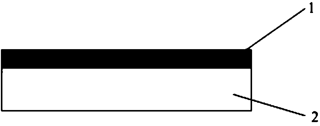
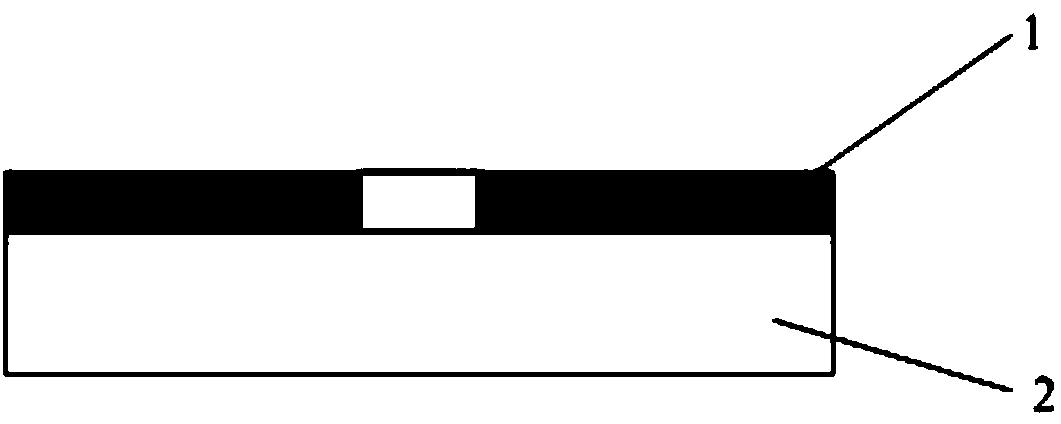
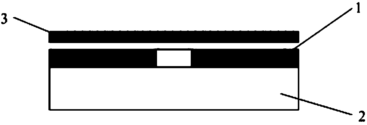
[0022] The present invention first forms SiO with a thickness of 300 nm on the Si substrate by thermal oxidation. 2 oxide layer, then the SiO 2 For surface pretreatment, bake in an oven at 150-200°C for 15-30 minutes to keep the surface dry and clean, and apply a layer of HMDS chemical adhesion enhancer to prevent it from falling off. Uniformly spin-coat photoresist and dry photoresist to cure the glue, then expose and develop to realize pattern transfer. SiO on non-spin-coated photoresist 2 The step of forming small holes by etching on the surface: using reactive ion etching method, on SiO without spin-coated photoresist 2 The surface is etched to form a 250nm deep hole with a diameter of 10um, and the photoresist is cleaned with acetone vapor, and then the sample is cleaned with ethanol and deionized water, such as figure 2 The schematic diagram of the hole structure is shown. The mechanical exfoliation method is used to prepare double-layer graphene using a special 3M ...


PUM


Abstract

The invention discloses a graphene field effect transistor, in particular to a preparation method of a graphene field effect transistor based on bubbling. The method includes the following steps: providing a substrate, and forming an oxide layer on the substrate; punching a hole in the oxide layer through photo-etching; forming a double-layer graphene channel through transfer above the hole; and putting the transferred graphene in a vacuum machine, carrying out vacuum pumping, carrying out inflation, and feeding nitrogen. According to the invention, the graphene suspended above the hole is compressed and vacuum-pumped in a vacuum pump under an airtight condition. The stress of graphene is increased. The switching ratio of the graphene field effect transistor is improved. The sensitivity characteristic of the field effect transistor is enhanced.

Description

technical field [0001] The invention relates to a graphene field effect transistor, in particular to a method for preparing a graphene field effect transistor based on a bubbling method. Background technique [0002] Graphene (Graphene) is a two-dimensional thin-film nanomaterial, and its basic atomic structure unit is a benzene ring structure composed of sp2 hybridized carbon atoms. This honeycomb-like hexagonal stable lattice structure makes graphene have good The optical and electrical properties of graphene and the compatibility of graphene with silicon-based semiconductor processes have attracted widespread attention from academia and industry. [0003] With the rapid development and continuous improvement of the semiconductor industry, the technology of the semiconductor industry has also made great progress. However, due to the prediction of Moore's Law, "the number of components that can be accommodated on an integrated circuit decreases approximately every 18-24 mon...

Claims


Application Information

Patent Timeline
Patent Type & Authority Applications(China)
IPC IPC(8): H01L21/336H01L21/28H01L21/683H01L29/06H01L29/423H01L29/51
CPCH01L29/66045H01L21/6836H01L29/0684H01L29/42364H01L29/513H01L29/517H01L2221/68386
Inventor 王权曾元明董金耀王江祥韦国成
Owner JIANGSU UNIV
Why Eureka
Try Eureka