

Technology and apparatus for producing aluminum alloy substrate printed circuit board
A technology of aluminum alloy substrate and printed circuit board, applied in printed circuit manufacturing, printed circuit, printed circuit components and other directions, can solve the problems of stability, poor reliability, performance degradation of electronic products, poor wettability of metal substrates, etc. Achieve the effect of improving efficiency, improving roughness, and excellent electrical performance
- Summary
- Abstract
- Description
- Claims
- Application Information
AI Technical Summary
Problems solved by technology
Method used
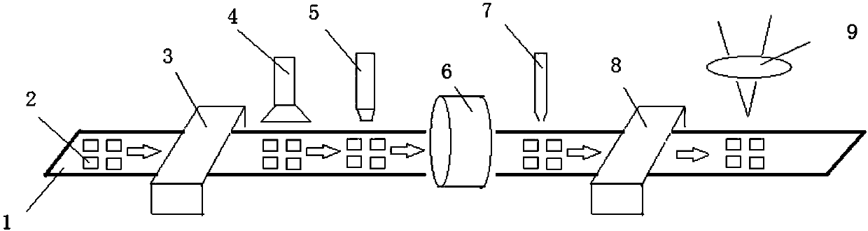
Image

Examples
Embodiment 1
[0030] Example 1: Preparation process of 2A16 aluminum alloy substrate printed circuit board
[0031] This embodiment provides a 2A16 aluminum alloy substrate printed circuit board preparation process, including the following steps:
[0032] First, put the 2A16 aluminum alloy substrate with a thickness of 0.5mm into the ultrasonic cleaning machine for rinsing, cleaning and drying;
[0033] Then, send the dried 2A16 aluminum alloy substrate into the first heating furnace (ordinary industrial electric furnace) to heat to 320°C and keep it warm for 8 minutes;
[0034] Next, take out the 2A16 aluminum alloy substrate. At this time, the temperature of the 2A16 aluminum alloy substrate is kept at about 300°C. A 30 μm aluminum coating is directly prepared on it by an arc spraying process. The surface roughness of the aluminum coating is 3 μm. Improve the bonding strength of the ceramic coating;
[0035] Secondly, a ceramic coating was prepared on the aluminum coating with a thickne...
Embodiment 2
[0041] Example 2: Preparation process of 3003 aluminum alloy substrate printed circuit board
[0042] This embodiment provides a 3003 aluminum alloy substrate printed circuit board preparation process, including the following steps:
[0043] First, put the 3003 aluminum alloy substrate with a thickness of 1mm into the ultrasonic cleaning machine for rinsing, cleaning and drying;
[0044] Then, send the dried 3003 aluminum alloy substrate into the first heating furnace, heat it to 330°C, and keep it warm for 5 minutes;
[0045] Next, take out the 3003 aluminum alloy substrate. At this time, the temperature of the 3003 aluminum alloy substrate is kept at about 310°C. A 30 μm aluminum coating is directly prepared on it by an arc spraying process. The surface roughness of the aluminum coating is 10 μm. Improve the bonding strength of the ceramic coating;
[0046] Secondly, the ceramic coating was prepared on the aluminum coating by plasma spraying method, with a thickness of 60 ...
Embodiment 3
[0051] Example 3: Preparation process of 4A01 aluminum alloy substrate PCB circuit board
[0052] This embodiment provides a 4A01 aluminum alloy substrate printed circuit board preparation process, including the following steps:
[0053] First, put the 4A01 aluminum alloy substrate with a thickness of 2mm into the ultrasonic cleaning machine for rinsing, cleaning and drying;
[0054] Then, send the dried 4A01 aluminum alloy substrate into an ordinary industrial electric furnace and heat it to 380°C for 2 minutes;
[0055] Secondly, take out the 4A01 aluminum alloy substrate. At this time, the temperature of the 4A01 aluminum alloy substrate is kept at about 300 ° C. A 30 μm aluminum coating is directly prepared on it by an arc spraying process. The surface roughness of the aluminum coating is 15 μm. Improve the bonding strength of the ceramic coating;
[0056] Secondly, a ceramic coating was prepared on the aluminum coating with a thickness of 40 μm by plasma spraying method...
PUM
| Property | Measurement | Unit |
|---|---|---|
| thickness | aaaaa | aaaaa |
| thickness | aaaaa | aaaaa |
| surface roughness | aaaaa | aaaaa |
Abstract
Description
Claims
Application Information