Fabrication method of high-band surface acoustic wave device electrode

A surface acoustic wave device and high-frequency technology, which is applied in the manufacture/assembly of piezoelectric/electrostrictive devices, etc., can solve the problems of preparation failure, consumption of EBL machine, difficulty in achieving preparation indicators, etc., to reduce resolution and The effect of yield rate, improvement of device temperature stability, and reduction of electron incident dose

Active Publication Date: 2018-04-13
NAT UNIV OF DEFENSE TECH
View PDF3 Cites 6 Cited by
  • Summary
  • Abstract
  • Description
  • Claims
  • Application Information

AI Technical Summary

Problems solved by technology

[0005] (2) The resolution of a single line of EBL can reach below 10nm, but the interdigitated electrode in the SAW device is a densely distributed metal line array, which is a high-resolution, high-density pattern, while the traditional EBL exposure is completed by point-by-point scanning. When the point-by-point scanning method is used for high-resolution dense graphics, the exposure dose is very large, and it will cause serious proximity effects, thereby limiting the resolution. Therefore, it is usually difficult for SAW device electrodes prepared by EBL technology to meet the preparation index;
[0006] (3) In order to reduce the exposure area and improve the efficiency, positive photoresist technology is usually used for exposure, but the hardness of this kind of photoresist is not high, especially when preparing high-resolution structures, it is easy to be affected by capillary action and collapse, resulting in failure of preparation and lower yield;
[0007] (4) SAW electrodes also include bus bars and pads. This type of structure is much larger than the size of interdigitated electrodes, often hundreds of microns. Therefore, the preparation of this large-scale electrode pattern will greatly consume EBL operation time and cost High but low economic benefits, output-to-input ratio is usually extremely low

Method used


Image

  • Fabrication method of high-band surface acoustic wave device electrode
  • Fabrication method of high-band surface acoustic wave device electrode
  • Fabrication method of high-band surface acoustic wave device electrode

Examples


Embodiment Construction

[0035] The present invention will be further described below in conjunction with the accompanying drawings and specific preferred embodiments, but the protection scope of the present invention is not limited thereby.

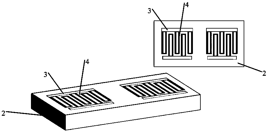
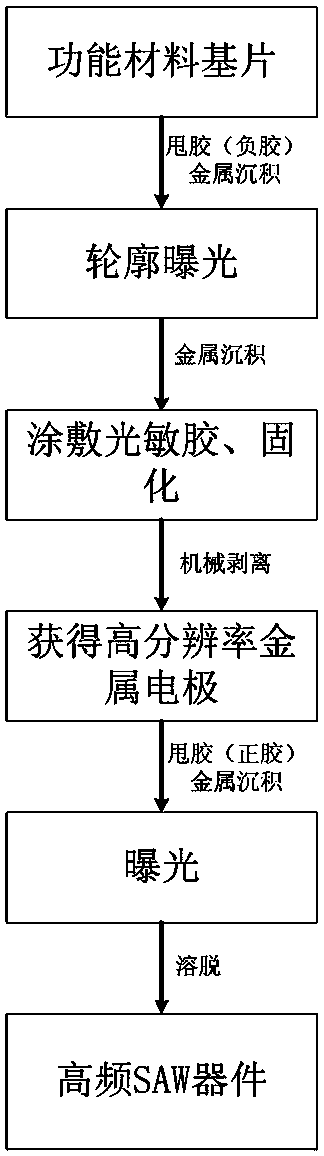
[0036] like figure 1 , 2 , 3, the preparation method of the electrode of the high-frequency surface acoustic wave device of the present embodiment, the steps include:

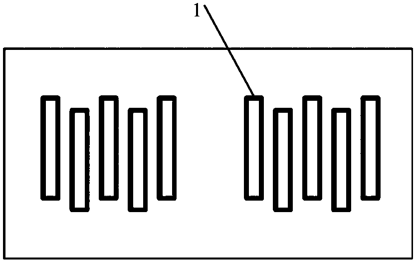
[0037] S1. On the substrate substrate of the piezoelectric functional material 2, use a negative adhesive to expose the outline of the interdigitated electrode in the electrode to be prepared;

[0038] S2. Metal deposition after exposure and development to obtain a metal coating with an outline pattern of interdigitated electrodes;

[0039] S3. Mechanically peel off the redundant metal layer outside the contour pattern to obtain the final dense pattern corresponding to the interdigitated electrodes;

[0040] S4. Use the positive resist to expose and metal-deposit the specified larger area of ​...


PUM


Abstract

The invention discloses a fabrication method of a high-band surface acoustic wave device electrode. The fabrication method comprises the steps of S1, exposing a profile of an interdigital electrode inan electrode to be fabricated on a substrate of a piezoelectric functional material by employing negative glue; S2, performing metal deposition after exposure and developing to obtain a metal coatinglayer with an interdigital electrode profile pattern; S3, mechanically stripping a redundant metal layer outside the profile pattern to obtain a final intensive pattern corresponding to the interdigital electrode; S4, performing exposure and metal deposition on a convergence bar and a bonding pad in the electrode to be fabricated by employing positive glue; and S5, stripping the redundant metal layer from the metal layer after being deposited by employing a solution removal process to obtain an electrode pattern corresponding to the convergence bar and the bonding pad so as to complete electrode fabrication. By the fabrication method, a nanoscale SAW device electrode compatible with a high-resolution intensive pattern and a large-size pattern can be obtained, and the fabrication method has the advantages of low cost, high fabrication efficiency, high yield, high SAW electrode quality, good universality and the like and is simple to implement and operate.

Description

technical field [0001] The invention relates to the technical field of micro-nano processing of nano-electronic components, in particular to a method for preparing electrodes of high-frequency surface acoustic wave devices. Background technique [0002] SAW (Surface Acoustic Wave, Surface Acoustic Wave) technology is widely used in cutting-edge scientific research and industrial equipment, such as signal processing, sensing, microwave communication, non-destructive testing, etc. Plays an important role in the field of quantum research. With the surge of information, improving the operating frequency of SAW devices has become a research hotspot. In order to increase the operating frequency of SAW devices, an important technical approach is to improve the resolution of the interdigital electrodes of the device. At present, the industry prepares high-resolution micro-nano pattern structures. Planar printing technology is used, and the process equipment includes mask exposure, ...

Claims


Application Information

Patent Timeline
Patent Type & Authority Applications(China)
IPC IPC(8): H01L41/29
CPCH10N30/06
Inventor 陈书明王磊张金英宁希池雅庆陈哲刘婧恬
Owner NAT UNIV OF DEFENSE TECH
Why Eureka
Try Eureka