Method for preparing silicon nanocrystalline with optical gain which can be improved by high-pressure hydrogen passivation
What is AI technical title?
AI technical title is built by PatSnap AI team. It summarizes the technical point description of the patent document.
A silicon nanocrystal, high-pressure hydrogen technology, applied in chemical instruments and methods, nanotechnology, inorganic chemistry, etc., can solve the problems of destroying the structure of the light-emitting layer, increasing the quenching center, structural defects, etc., to achieve the effect of improving light gain
Inactive Publication Date: 2018-05-11
FUDAN UNIV
View PDF5 Cites 6 Cited by
Summary
Abstract
Description
Claims
Application Information
AI Technical Summary
This helps you quickly interpret patents by identifying the three key elements:
Problems solved by technology
Method used
Benefits of technology
Problems solved by technology
However, there are some defects in these methods: the high temperature annealing method has certain obstacles to the formation of silicon-hydrogen bonds, so its effect on improving luminescence is limited; the high-energy hydrogen ion implantation method will destroy the structure of the light-emitting layer, introduce structural defects, and increase quenching centers; The bulk discharge method requires the activation of hydrogen by discharge
Method used
Image
Click on the blue label to locate the original text in one second.
Reading with bidirectional positioning of images and text.
PUM
Abstract
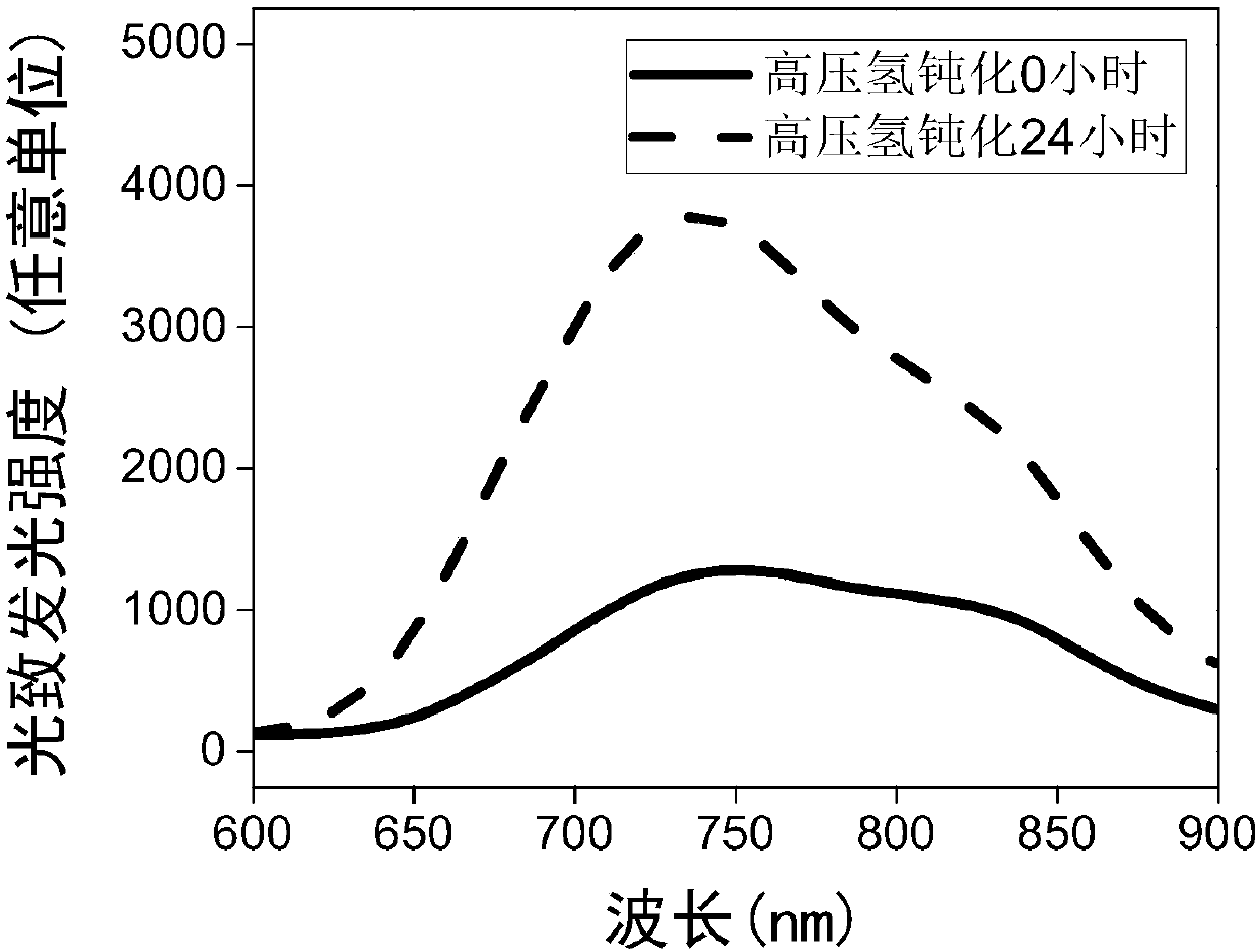
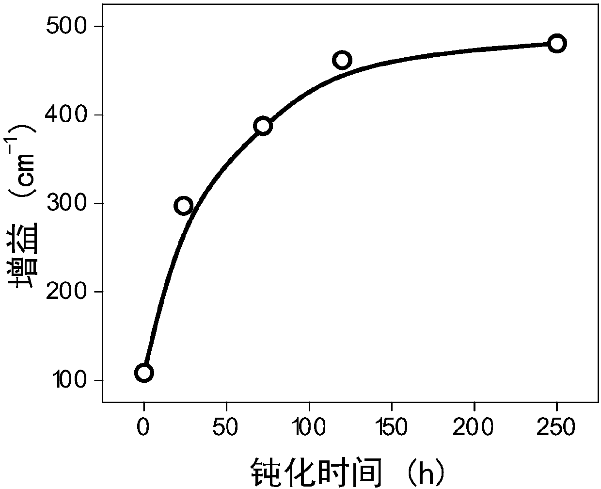
The invention specifically relates to a method for preparing silicon nanocrystalline with optical gain which can be improved by high-pressure hydrogenpassivation. According to the method provided bythe invention, in virtue of the hydrogenpassivation principle which is common in the field of semiconductor electronic circuits, hydrogen is used as a basic raw material for material treatment, and the means of proper heating and high-pressure sealing are used, so that material passivation is realized. The silicon nanocrystalline is used as a whole siliconluminescent material, and a large numberof defect centers can be produced in the preparation process of the silicon nanocrystalline. Part of defects in a luminescent material can be effectively saturated and eliminated through the high-pressure hydrogen passivation, and the non-radiation recombination centers are reduced, so that the effects of remarkably increasing the luminous intensity and the optical gain of the nanocrystalline silicon can be realized, and thus the nano crystalline silicon material with improved optical gain can be used for developing a novel silicon laser. The invention provides the hydrogen passivation methodwhich is different from conventional high-temperature hydrogen passivation and plasma hydrogen passivation, and according to the process, high temperature does not need to be maintained, the plasmadischarge process is not needed, the luminescence enhancing effect on the material is remarkable, the cost is low, the operation is simple, and the process is safe and controllable.
Description
technical field [0001] The invention belongs to the field of new materials, and in particular relates to a method for preparing silicon nanocrystals with high-pressure hydrogen passivation to improve light gain. Background technique [0002] In the early 1990s, Canham, UK, discovered that porous silicon has photoluminescent properties. Since then, the study of nanoscale silicon materials has set off a whole research upsurge. Due to its own indirect bandgap energy band characteristics, the probability of spontaneous emission at room temperature to produce light is very low. It is generally believed that the photoluminescence phenomenon of silicon nanocrystals is caused by the quantum confinement effect. Silicon nanocrystals wrapped in a medium are favored by everyone because of their firm structure and stable luminescence, and they also have the property of changing their luminescence peak position by adjusting their size. There are many ways to prepare silicon nanocrystal...
Claims
Application Information
Patent Timeline
Application Date:The date an application was filed.
Publication Date:The date a patent or application was officially published.
First Publication Date:The earliest publication date of a patent with the same application number.
Issue Date:Publication date of the patent grant document.
PCT Entry Date:The Entry date of PCT National Phase.
Estimated Expiry Date:The statutory expiry date of a patent right according to the Patent Law, and it is the longest term of protection that the patent right can achieve without the termination of the patent right due to other reasons(Term extension factor has been taken into account ).
Invalid Date:Actual expiry date is based on effective date or publication date of legal transaction data of invalid patent.

