

Low-power AlGaInP red light semiconductor laser with superlattice electron barrier layer and preparation method of low-power AlGaInP red light semiconductor laser
An electronic blocking layer and superlattice technology, applied in the field of optoelectronics, can solve the problems of large light absorption, no stress compensation involved, and low slope efficiency, etc., and achieve the effects of increasing optical gain, reducing heat generation, and improving slope efficiency
- Summary
- Abstract
- Description
- Claims
- Application Information
AI Technical Summary
Problems solved by technology
Method used
Image

Examples
Embodiment 1
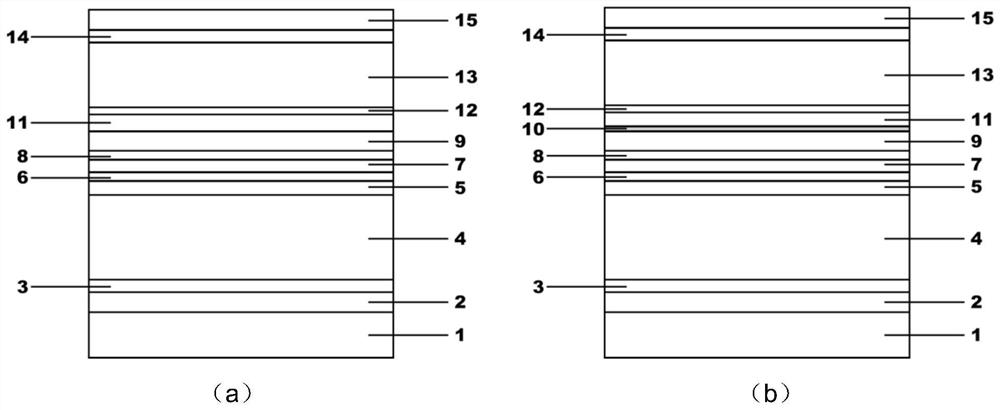
[0081] A method for preparing a low-power AlGaInP red semiconductor laser with a superlattice electron blocking layer, comprising the following steps:
[0082] S1, put the GaAs substrate in the growth chamber of the MOCVD equipment, H 2 Bake at 720±10°C under ambient conditions; and pass AsH 3 , performing surface heat treatment on the GaAs substrate;
[0083] S2, slowly lower the temperature to 680±10°C, the cooling rate is not higher than 30°C / min, and feed TMGa and AsH 3 , grow a GaAs buffer layer on a GaAs substrate; the doping source of the GaAs buffer layer is Si 2 h 6 , the doping concentration of Si atoms is 2×10 18 atoms / cm 3 , the thickness of the GaAs buffer layer is 0.2 μm.
[0084] S3, keep the temperature at 680±10°C, pass PH 3 , by aborting the passage of AsH 3 and TMGa to realize the growth pause of the GaAs buffer layer, and pause for 5s to deplete the As atoms in the reaction chamber.
[0085] S4, keep the temperature at 680±10°C, pass through TMGa, ...
Embodiment 2
[0101] A method for preparing a low-power AlGaInP red semiconductor laser with a superlattice electron blocking layer, comprising the following steps:
[0102] S1, put the GaAs substrate in the growth chamber of the MOCVD equipment, H 2 Bake at 720±10°C under ambient conditions; and pass AsH 3 , performing surface heat treatment on the GaAs substrate;
[0103] S2, slowly lower the temperature to 680±10°C, the cooling rate is not higher than 30°C / min, and feed TMGa and AsH 3 , grow a GaAs buffer layer on a GaAs substrate; the doping source of the GaAs buffer layer is Si 2 h 6 , the doping concentration of Si atoms is 2.5×10 18 atoms / cm 3 , the thickness of the GaAs buffer layer is 0.15 μm.
[0104] S3, keep the temperature at 680±10°C, pass PH 3 , by aborting the passage of AsH 3 and TMGa to realize the growth pause of the GaAs buffer layer, and the pause is 10s to deplete the As atoms in the reaction chamber.
[0105] S4, keep the temperature at 680±10°C, pass through...
PUM
| Property | Measurement | Unit |
|---|---|---|
| Thickness | aaaaa | aaaaa |
| Thickness | aaaaa | aaaaa |
| Thickness | aaaaa | aaaaa |
Abstract
Description
Claims
Application Information