Large-area CVD graphene doping and transferring method
A transfer method, graphene technology, applied in graphene, chemical instruments and methods, inorganic chemistry, etc., can solve problems affecting graphene quality, continuous graphene film wrinkles, and low mechanical strength of PMMA film, etc., to achieve high efficiency and uniformity Effects of stabilizing doping, inhibiting dopant migration, and ensuring transfer integrity
- Summary
- Abstract
- Description
- Claims
- Application Information
AI Technical Summary
Problems solved by technology
Method used
Image
Examples
Embodiment 1
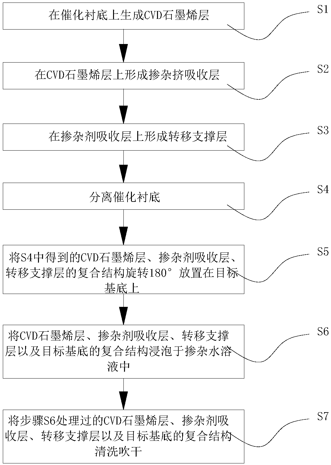
[0056] S1. Generate a CVD graphene layer 201 with a two-dimensional continuous structure on the copper foil of the catalytic substrate 101 by the CVD method to obtain a composite structure of copper foil and graphene layer;
[0057] S2. Mix the resin with the main chain of polyethylene oxide and the end group of acrylate with the bifunctional acrylate monomer, and coat it on the CVD graphene layer 201 obtained in step S1, and cure by ultraviolet light irradiation to form a doped Miscellaneous agent absorption layer 301. The formed dopant absorption layer 301 has a thickness of 3 μm, a cross-linking degree of 40%, and a saturated swelling degree in water of 10%;
[0058] S3. Depositing a transfer support layer 302 made of poly 2,5-dichloro-para-xylene on the dopant absorption layer 301 formed in step S2 at a temperature of 40°C by the CVD method, with a thickness of 5 μm, and water vapor permeable Over rate is 0.3g / (m 2 ·Day);
[0059] S4. Separate the copper foil catalytic substrat...
Embodiment 2
[0068] S1. Generate a graphene layer with a two-dimensional continuous structure on the copper foil of the catalytic substrate 101 by the CVD method to obtain a composite structure of copper foil / graphene layer;
[0069] S2. Mixing polyvinyl alcohol and diisocyanate, coating on the CVD graphene layer 201 obtained in step S1, and curing by heating to form a dopant absorption layer 301. The formed dopant absorption layer 301 has a thickness of 1 μm, a crosslinking degree of 60%, and a saturated swelling degree in water of 1%;
[0070] S3. Depositing a transfer support layer 302 made of parylene on the dopant absorption layer 301 formed in step S2 at a temperature of 40°C by the CVD method with a thickness of 0.5μm and a water vapor transmission rate of 0.9g / (m 2 ·Day);
[0071] S4. Separate the copper foil catalytic substrate 101 to obtain a composite structure of a CVD graphene layer 201, a cross-linked polyvinyl alcohol dopant absorption layer 301, and a parylene transfer support l...
Embodiment 3
[0080] S1. Generate a VCD graphene layer 201 with a two-dimensional continuous structure on the copper foil of the catalytic substrate 101 by the CVD method to obtain a composite structure of copper foil / graphene layer;
[0081] S2. Mixing methyl cellulose and diisocyanate, coating on the CVD graphene layer 201 obtained in step S1, and curing by heating to form a dopant absorption layer 301. The formed dopant absorbing layer 301 has a thickness of 0.1 μm, a cross-linking degree of 50%, and a saturated swelling degree in water of 4%;
[0082] S3. Depositing a transfer support layer 302 made of poly-3-chloroparaxylene on the dopant absorption layer 301 formed in step S2 at a temperature of about 40°C by the CVD method, with a thickness of 1 μm, and a water vapor transmission rate 0.8g / (m 2 ·Day);
[0083] S4. Separate the copper foil catalytic substrate 101 to obtain a composite structure of a CVD graphene layer 201, a cross-linked cellulose dopant absorption layer 301, and a poly-3-c...
PUM
| Property | Measurement | Unit |
|---|---|---|
| Thickness | aaaaa | aaaaa |
| Thickness | aaaaa | aaaaa |
| Thickness | aaaaa | aaaaa |
Abstract
Description
Claims
Application Information


