High-quality AlN epitaxial film, preparation method of high-quality AlN epitaxial film and application of high-quality AlN epitaxial film

An epitaxial thin film, lateral epitaxy technology, applied in the direction of final product manufacturing, sustainable manufacturing/processing, semiconductor/solid-state device manufacturing, etc. Atomic level flatness and other problems, to achieve the effect of low dislocation density, elimination of cracks, and smooth surface

Inactive Publication Date: 2018-06-12
北京中博芯半导体科技有限公司
View PDF5 Cites 23 Cited by
  • Summary
  • Abstract
  • Description
  • Claims
  • Application Information

AI Technical Summary

Problems solved by technology

Although these methods can improve the crystal quality of AlN epitaxial films to a certain extent, it is often difficult to obtain AlN epitaxial films that are completely crack-free, atomically flat, and have low dislocation density at the same time with high repeatability.
[0005] There are also methods in the prior art that can prepare AlN epitaxial thin films that are completely crack-free, atomically flat, and have low dislocation density, but they often have the disadvantages of narrow process window and poor repeatability
In addition, although the preparation of AlN substrates by physical vapor transport (PVT), or the homogeneous epitaxy scheme prepared by PVT combined with hydride vapor phase epitaxy (HVPE), can better achieve the above goals, but the cost is too high, and the size of AlN Defects that are too small to be industrially produced on a large scale

Method used


Image

  • High-quality AlN epitaxial film, preparation method of high-quality AlN epitaxial film and application of high-quality AlN epitaxial film
  • High-quality AlN epitaxial film, preparation method of high-quality AlN epitaxial film and application of high-quality AlN epitaxial film
  • High-quality AlN epitaxial film, preparation method of high-quality AlN epitaxial film and application of high-quality AlN epitaxial film

Examples


Embodiment 1

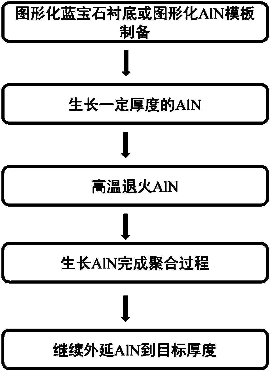
[0048] Embodiment 1 (taking the preparation of sapphire substrate as an example)

[0049] S1: Prepare a concave patterned sapphire substrate, the specific steps are:

[0050] 1) First use PECVD to deposit SiO with a thickness of 200nm on a 2-inch c-plane sapphire substrate 2 , and then spin coat TU7-220 glue with a thickness of 300nm.

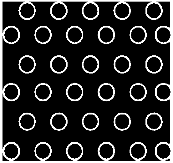
[0051] 2) Using a nano imprinter The pattern transfer polymer on the embossing template (the table size is 400nm) with a period of 1.2 microns and a circular hole diameter of 800nm ​​is placed on the polymer, and then the pattern on the polymer is embossed on the embossing glue under the condition of ultraviolet exposure.

[0052] 3) Using ICP to transfer the pattern to SiO with imprinting glue as a mask 2 superior.

[0053] 4) with SiO 2 Use H as a mask 2 SO 4 and H 3 PO 4 The mixed solution corrodes the sapphire at a temperature of 270°C, and transfers the pattern to the sapphire substrate.

[0054] 5) The remaining SiO on the sapp...

Embodiment 2

[0060] Example 2 (taking growth on a concave patterned AlN template as an example)

[0061] S1: Prepare a concave AlN template substrate, the specific steps are:

[0062] 1) Prepare an AlN template with a thickness of 1 micron using MOCVD equipment (3×2”Aixtron CCS FP-MOCVD). SU8 glue is placed on the AlN template with a thickness of 600nm.

[0063] 2) Using a nano imprinter The pattern transfer polymer on the embossing template (the mesa size is 350nm) with a period of 1 micron and a circular hole diameter of 650nm is placed on the polymer, and then the pattern on the polymer is embossed on the embossing glue under the condition of ultraviolet exposure.

[0064] 3) ICP is used to transfer the embossing glue as a mask pattern to the AlN template, and the hole depth is 300 nanometers.

[0065] 4) Remove the remaining SU8 glue on the AlN template with acetone to obtain a nanopatterned AlN template, and thoroughly clean the substrate and dry it.

[0066] S2: Place the prepare...


PUM

PropertyMeasurementUnit
thicknessaaaaaaaaaa
thicknessaaaaaaaaaa

Abstract

The invention relates to a high-quality AlN epitaxial film, a preparation method of the high-quality AlN epitaxial film and the application of the high-quality AlN epitaxial film. According to the invention, the two core links of imaging a sapphire substrate / AlN template and carrying out the high-temperature annealing are combined. The approach of effectively reducing the residual stress is realized through the lateral epitaxy process and the high-temperature annealing process. In this way, an AlN epitaxial film, which is free of cracks, flat in atom level and low in dislocation density, is obtained. As a result, the invention has important significance for realizing the industrial application of AlGaN-based deep ultraviolet high-performance light-emitting and detecting instruments.

Description

technical field [0001] The invention relates to an AlN epitaxial film with no cracks, atomic-level flat surface and low dislocation density, its preparation method and application, and belongs to the technical field of preparation of Group III nitride semiconductors. Background technique [0002] AlGaN with high Al composition and its low-dimensional quantum structure optoelectronic functional materials are irreplaceable material systems for the preparation of solid-state deep ultraviolet (DUV) optoelectronic devices. The field has a wide range of applications and is one of the most promising fields and industries for III-nitride semiconductors. Since the Chinese government has signed to participate in the "Minamata Convention", the international production and trade of mercury-containing products will be banned in 2020. Therefore, the development of high-performance AlGaN-based solid-state DUV-LED light sources has become a more urgent task. [0003] Due to the current int...

Claims


Application Information

Patent Timeline
Patent Type & Authority Applications(China)
IPC IPC(8): H01L21/205H01L33/00H01L33/32H01L31/18H01L31/0304
CPCH01L21/0243H01L21/0254H01L21/0262H01L21/02656H01L31/03044H01L31/1852H01L31/1856H01L33/007H01L33/32Y02P70/50
Inventor 许福军沈波解楠王明星孙元浩刘百银秦志新
Owner 北京中博芯半导体科技有限公司
Why Eureka
Try Eureka