Photocathode based on novel nanostructure and preparation method thereof

A nanostructure and photocathode technology, which is applied in the manufacture of light-emitting cathodes, photoemission cathodes, nanotechnology for materials and surface science, etc., can solve problems such as reducing the emission current, achieve lower thresholds, enhance local electric fields, and conduct electricity. The effect of high sex and electron mobility

Active Publication Date: 2018-06-29
SOUTHEAST UNIV
View PDF7 Cites 13 Cited by
  • Summary
  • Abstract
  • Description
  • Claims
  • Application Information

AI Technical Summary

Problems solved by technology

[0005] Since the field electron emission regions of aligned carbon nanotubes are mainly concentrated in their edge regions, the shielding effect will be generated between the dense carbon nanotube arrays, thereby reducing the total emission current.

Method used


Image

  • Photocathode based on novel nanostructure and preparation method thereof
  • Photocathode based on novel nanostructure and preparation method thereof
  • Photocathode based on novel nanostructure and preparation method thereof

Examples


Embodiment 1

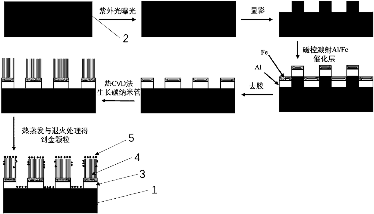
[0032] see Figure 1 to Figure 3 , the present invention provides a novel nanostructured photocathode, the novel nanostructured photocathode is formed on a substrate 1, the novel nanostructured photocathode comprises a patterned catalytic layer 3, a catalyst layer formed on the catalytic layer 3 Patterned carbon nanotubes 4 and modified metal particles 5 formed on the carbon nanotubes 4 . In addition, the lower surface of the substrate 1 is coated with conductive silver paste or gallium indium solder as a cathode electrode.

[0033] In this embodiment, the material of the substrate 1 is preferably a heavily doped n-type silicon wafer, but it is not limited thereto, and may also be, for example, other types of silicon wafers or a quartz substrate with a transparent conductive layer. The lower surface of the substrate 1 is coated with conductive silver paste or gallium indium solder as a cathode electrode, and the anode uses indium tin oxide (ITO) transparent conductive glass o...

Embodiment 2

[0039] The invention provides a preparation method for the novel nanostructure photocathode of the present invention, see Figure 1 to Figure 3 , the nanostructured photocathode of the present invention is prepared on a substrate material, such as a silicon wafer or a quartz substrate with a transparent conductive layer. In this embodiment, the substrate material is a heavily doped n-type silicon wafer , its specific preparation method is as follows:

[0040] (1) Cleaning of the silicon substrate:

[0041] For example, immerse in diluted HF solution to remove surface oxides, and then use acetone, alcohol and deionized water to clean the surface sequentially with ultrasonic cleaning.

[0042] (2) Photolithography:

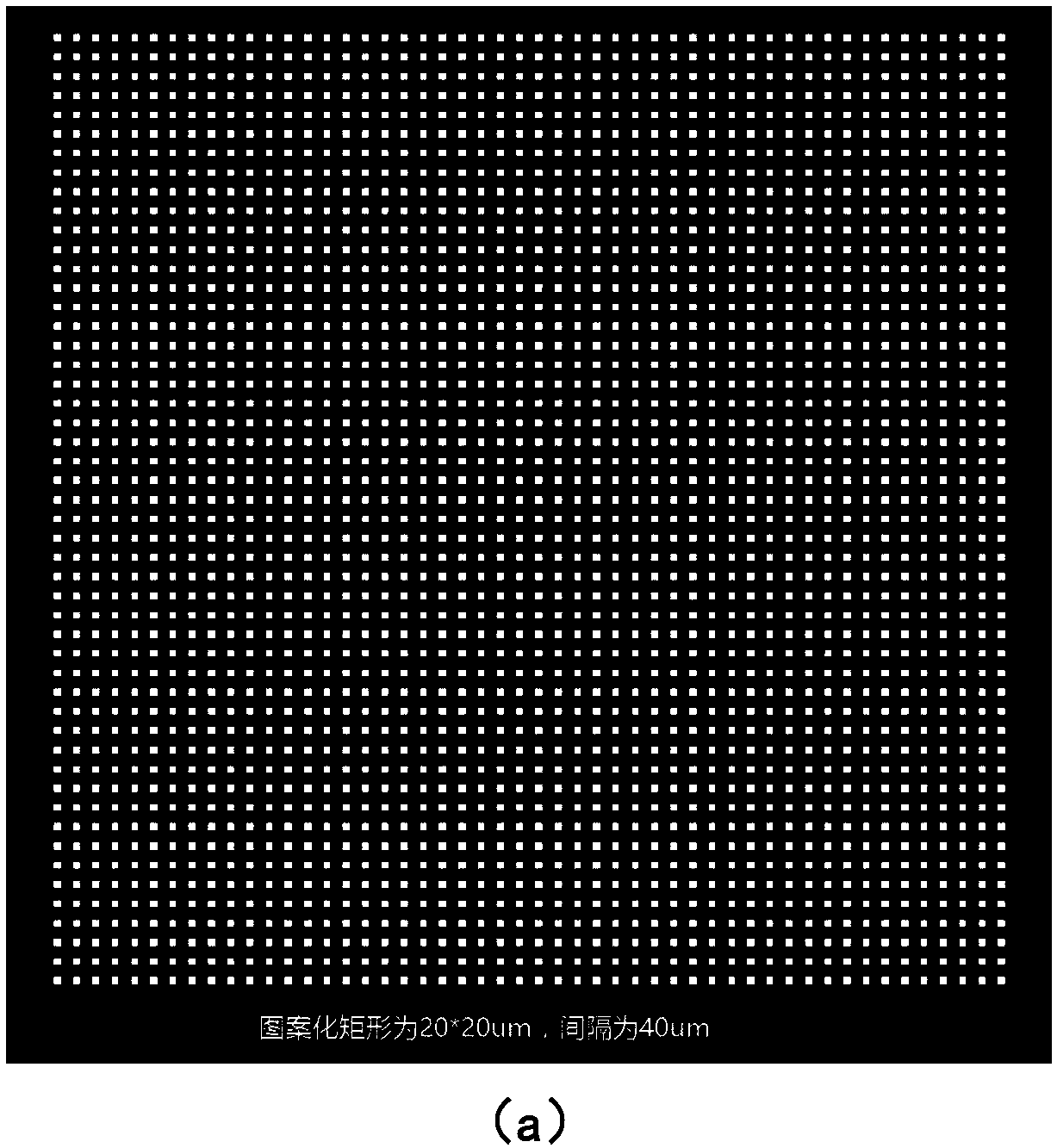
[0043] Use a spin coater to pre-rotate the photoresist (positive resist) at 1000r / min for 15s, then pre-rotate at 5000r / min for 60s; bake the spin-coated silicon wafer at 110°C for 90s before cooling; put the mask plate (see figure 2 (a)) Cover the photoresist ...


PUM

PropertyMeasurementUnit
thicknessaaaaaaaaaa
thicknessaaaaaaaaaa
sizeaaaaaaaaaa

Abstract

The invention provides a novel nanostructure photocathode which comprises a patterned catalytic layer, a patterned vertical carbon nanotube formed on the catalytic layer and a metal nanoparticle witha plasmon effect modified on the vertical carbon nanotube. The invention further provides a preparation method of the novel nanostructure photocathode. The novel nanostructure photocathode and the preparation method provided by the invention have the benefits that an electrostatic shielding effect on the cathode surface can be effectively prevented through the patterning treatment of a cathode electron emission material, and a fringe effect is fully utilized, so that a cathode surface barrier is compressed, and a threshold of light energy required for electron emission is lowered; the carbon nanotube and the metal nanoparticle are combined, so that the excellent electrical performance and the environmental stability of the carbon nanotube are utilized, and meanwhile, a surface plasmon resonance effect of the metal nanoparticle is also utilized. Therefore, the enhancement of a light wave local electric field and the photon absorption enhancement can be realized.

Description

【Technical field】 [0001] The invention relates to a novel nanostructure photocathode combining patterned carbon nanotubes and metal nano-nanoparticles, an electric field-assisted photocathode and a preparation process and method thereof, mainly utilizing the excellent electron emission of carbon nanotubes, and applying The invention relates to an electron source and belongs to the technical field of optoelectronic devices. 【Background technique】 [0002] There are three basic principles for cathode emission of electrons so far. 1. Thermionic emission, that is, the use of elevated temperature to give electrons enough energy to make them jump out of the surface of the cathode. Hot cathodes are currently mainly used in various high-power microwave devices, but they have low efficiency, slow response and large emission angles. 2. Field electron emission, that is, applying a strong electric field on the surface of an object reduces the surface barrier and accelerates electrons,...

Claims


Application Information

Patent Timeline
Patent Type & Authority Applications(China)
IPC IPC(8): H01J1/34H01J9/12B82Y30/00B82Y40/00
CPCB82Y30/00B82Y40/00H01J1/34H01J9/12
Inventor 王琦龙徐林齐志央田润知张建张晓兵屠彦
Owner SOUTHEAST UNIV
Why Eureka
Try Eureka