Manufacturing process of vertical ceramic patch capacitor and capacitor product of vertical ceramic patch capacitor

A chip capacitor and manufacturing process technology, applied in the field of microelectronics, can solve problems such as inapplicability of vertical capacitors, worrying about the efficiency and accuracy of chip loading, and installation troubles, so as to save equipment and manpower investment and be compatible with automatic installation processes , the effect of ensuring integrity

Inactive Publication Date: 2018-07-13
SHANDONG DIYI ELECTRONICS SCI & TECH
View PDF4 Cites 16 Cited by
  • Summary
  • Abstract
  • Description
  • Claims
  • Application Information

AI Technical Summary

Problems solved by technology

[0002] SMD capacitor is a mature microelectronic passive device, which is mostly used for energy storage or filtering on circuits. However, when the existing MLCC capacitor is used in flat package components, its shape and terminal electrode form are not suitable for components in the package. The vertical installation method causes troubles to the application of capacitors in package components, and the trouble caused by MLCC capacitors to installation: the automatic installation of devices in package components is carried out, while the shape of conventional MLCC capacitors is narrow and flat, such as Figure 7 As shown, the upper surface is narrow and slender, and the surface is uneven due to the bulging of the electrodes at both ends, resulting in an extremely low capture rate in the automated welding process, resulting in a low yield rate in automated production. ...

Method used


Image

  • Manufacturing process of vertical ceramic patch capacitor and capacitor product of vertical ceramic patch capacitor
  • Manufacturing process of vertical ceramic patch capacitor and capacitor product of vertical ceramic patch capacitor
  • Manufacturing process of vertical ceramic patch capacitor and capacitor product of vertical ceramic patch capacitor

Examples


Embodiment 1

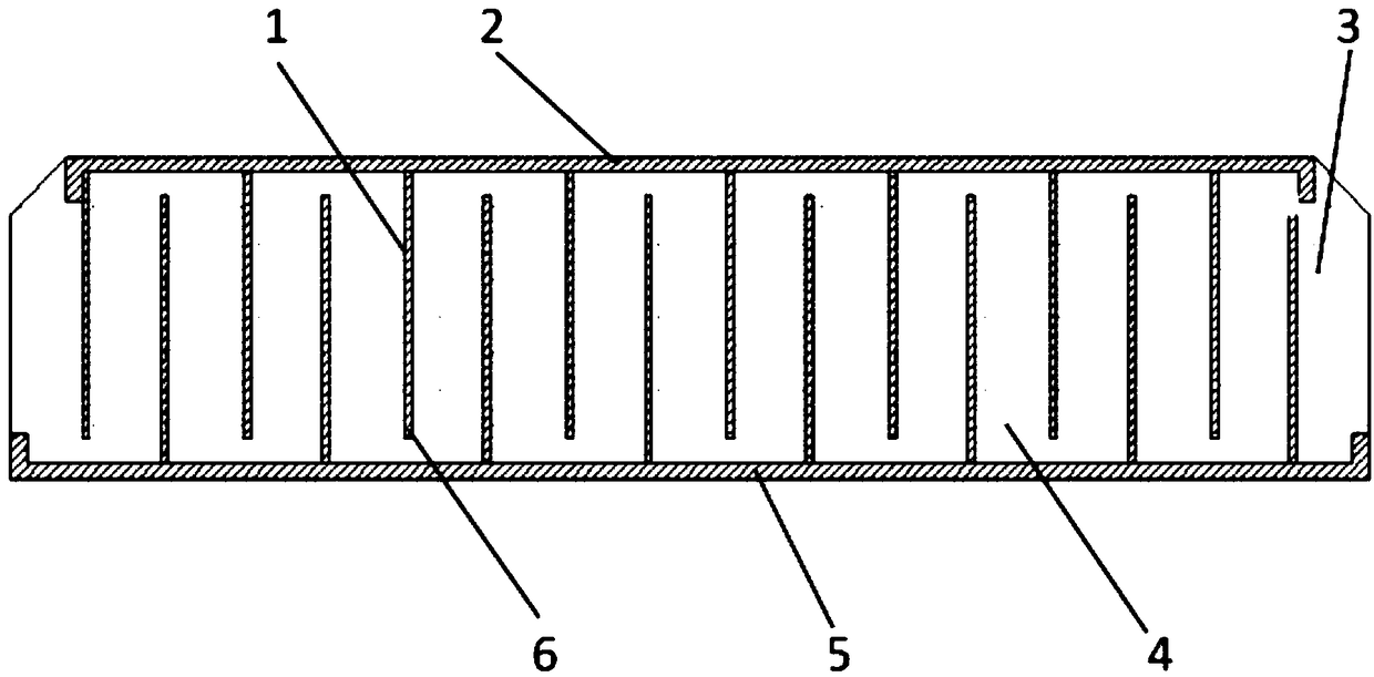
[0044] Such as figure 1 As shown, the construction principle of the vertical ceramic chip capacitor is that the upper and lower inner electrodes 6 are separated by dielectric ceramics to store and release electric energy in the form of static electricity. The capacity formula is as follows:

[0045]

[0046] C: Capacitance; ε: Dielectric constant of the insulator between electrodes; K: Dielectric constant (depending on the type of ceramic)

[0047] A: conductive area; D: thickness of dielectric layer 4 (thin strip thickness); n: number of layers (number of stacked layers);

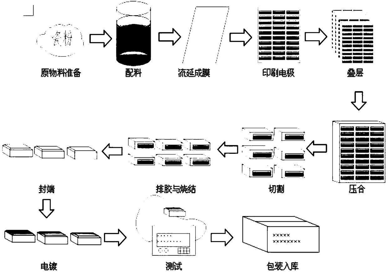
[0048] The manufacturing process of the vertical ceramic patch capacitor of the present invention comprises the following steps:

[0049] 1) Ingredients: The main raw material barium titanate (BaTiO3) base powder is mixed with the corresponding binder, solvent, and additives according to the formula, and stirred evenly to form a ceramic slurry; the ratio of each ingredient will change due to the capac...

Embodiment 2

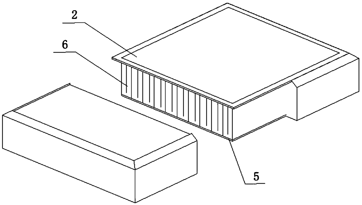
[0065] like Figure 2-4 As shown, the vertical ceramic chip capacitor of the present invention includes a capacitor body 3, and the capacitor body 3 includes an upper end face 2 and a lower end face 5, and internal electrodes 6 are arranged on the inner sides of the upper end face 2 and the lower end face 5, and the inner electrodes 6 includes an upper electrode and a lower electrode, the upper electrode and the lower electrode are vertically staggered, and one end of the upper electrode is connected to the upper end surface 2, and the other end does not touch the lower end surface 5, and the lower electrode is connected to the lower end surface 5, and the other end does not touch the upper end surface 2 , The upper end surface 2 and the lower end surface 5 are provided with a metal layer to form an external terminal electrode 7 , and the terminal electrode 7 is parallel to the mounting surface and connected to the internal electrode 6 .

[0066] In order to further illustrate...


PUM

PropertyMeasurementUnit
Thicknessaaaaaaaaaa

Abstract

The invention discloses a manufacturing process of a vertical ceramic patch capacitor and a capacitor product of the vertical ceramic patch capacitor, and belongs to the technical field of microelectronics. The process comprises the steps of material preparation, in which raw materials are mixed according to a proportion; coating, in which a layer of uniform paste thin film is formed from paste bya coating machine; printing, in which internal electrode paste is printed onto a ceramic film by a screen printing plate according to the process requirement; lamination, in which the printed ceramicfilms are laminated to form green blank having different layers; lamination, in which the green blank is loaded in a lamination bag; cutting, in which the laminated large green blank is cut to relatively small blanks; gluing, in which the cut blank blocks are glued; sintering, in which the green blank is sintered to form a ceramic body; chamfering, corners of the product of the capacitor sinteredto form ceramic are chamfered; sealing, in which the product is sealed to form the ceramic body; and sintering, in which the ceramic body is sintered to form the ceramic capacitor. The purpose of changing the shape of the capacitor and the electrode direction is achieved by changing an electrode printing method, a cutting method and a coating process, so that the installation and the applicationof a capacitor in a flat package component can be adapted.

Description

technical field [0001] The invention relates to a manufacturing process of a vertical ceramic chip capacitor and a capacitor product thereof, belonging to the technical field of microelectronics. Background technique [0002] SMD capacitor is a mature microelectronic passive device, which is mostly used for energy storage or filtering on circuits. However, when the existing MLCC capacitor is used in flat package components, its shape and terminal electrode form are not suitable for components in the package. The vertical installation method causes troubles to the application of capacitors in package components, and the trouble caused by MLCC capacitors to installation: the automatic installation of devices in package components is carried out, while the shape of conventional MLCC capacitors is narrow and flat, such as Figure 7 As shown, the upper surface is narrow and slender, and the surface is uneven due to the bulging of the electrodes at both ends, resulting in an extrem...

Claims


Application Information

Patent Timeline
IPC IPC(8): H01G4/30H01G4/232H01G4/012H01G4/224H01G13/00H01G4/12
CPCH01G4/306H01G4/012H01G4/1227H01G4/224H01G4/232H01G4/2325H01G13/00H01G13/003H01G13/006
Inventor 李明芬吴南吕敏李联勋马东平王鹏
Owner SHANDONG DIYI ELECTRONICS SCI & TECH
Why Eureka
Try Eureka