Charge-coupled device based on two-dimensional material films/insulating layers/semiconductor structures

A charge-coupled device and material thin film technology, applied in the field of image sensors, can solve problems such as difficulty in controlling CCD yield, data cannot be transmitted normally, and response speed is slow, so as to improve quantum efficiency, reduce dark current, and reduce noise.

Inactive Publication Date: 2018-07-13
杭州紫元科技有限公司
View PDF9 Cites 6 Cited by
  • Summary
  • Abstract
  • Description
  • Claims
  • Application Information

AI Technical Summary

Problems solved by technology

Compared with CMOS image sensors, the traditional CCD has better imaging quality, but because the CCD uses the way of horizontal charge transfer between pixels to output data, the overall response speed of the system is slow, and as long as one of the pixel transfer fails, it will As a result, a whole row of data cannot be transmitted normally, so it is difficult to control the yield rate of CCD

Method used


Image

  • Charge-coupled device based on two-dimensional material films/insulating layers/semiconductor structures
  • Charge-coupled device based on two-dimensional material films/insulating layers/semiconductor structures
  • Charge-coupled device based on two-dimensional material films/insulating layers/semiconductor structures

Examples


Embodiment 1

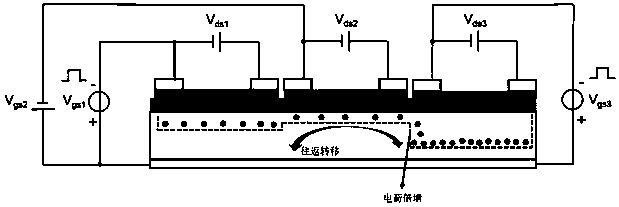
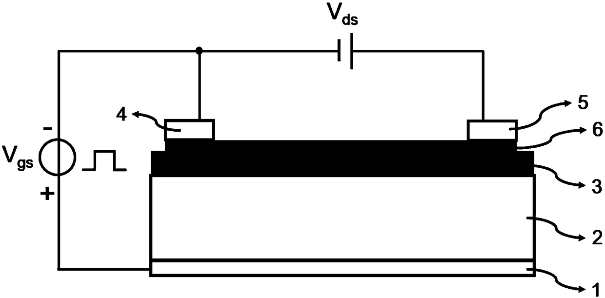
[0035] Depend on figure 1 As shown, a charge-coupled device based on a two-dimensional material thin film / insulating layer / semiconductor structure in this embodiment includes several pixels forming an array, and the pixels sequentially include a gate 1, a semiconductor substrate 2, and an insulating layer from bottom to top. 3. Graphene film 6, source 4 and drain 5; graphene film 6 covers the upper surface of insulating layer 3; source 4 and drain 5 are horizontally arranged on the upper surface of graphene film 6, and graphene film 6 has photoelectric response and field effect at the same time.

[0036] Among them, the material for making the gate 1 is gallium indium alloy, the thickness of the semiconductor substrate 2 is 300-500 μm, the resistivity is 1-10 Ω·cm, the thickness of the insulating layer 3 is 10-100 nm, the source 4 and the drain 5 The material used is chromium / gold alloy, and the size of the graphene film 6 is 100 μm×100 μm.

[0037] A pulsed gate voltage is ...

Embodiment 2

[0047] Depend on figure 1 As shown, a charge-coupled device based on a two-dimensional material thin film / insulating layer / semiconductor structure in this embodiment includes several pixels forming an array, and the pixels sequentially include a gate 1, a semiconductor substrate 2, and an insulating layer from bottom to top. 3. Black phosphorus film 6, source electrode 4 and drain electrode 5; black phosphorus film 6 covers the upper surface of insulating layer 3; source electrode 4 and drain electrode 5 are horizontally arranged on the upper surface of black phosphorus film 6, and black phosphorus film 6 has photoelectric response and field effect at the same time.

[0048] Among them, the material for making the gate 1 is gallium indium alloy, the thickness of the semiconductor substrate 2 is 300-500 μm, the resistivity is 1-10 Ω·cm, the thickness of the insulating layer 3 is 10-100 nm, the source 4 and the drain 5 The material used is chromium / gold alloy, and the size of t...

Embodiment 3

[0054] Depend on figure 1 As shown, a charge-coupled device based on a two-dimensional material thin film / insulating layer / semiconductor structure in this embodiment includes several pixels forming an array, and the pixels sequentially include a gate 1 and a narrow bandgap semiconductor substrate 2 from bottom to top. , an insulating layer 3, a molybdenum disulfide film 6, a source 4 and a drain 5; the molybdenum disulfide film 6 covers the upper surface of the insulating layer 3; the source 4 and the drain 5 are horizontally arranged on the molybdenum disulfide film 6 On the upper surface, the molybdenum disulfide thin film 6 has photoelectric response and field effect at the same time.

[0055] Among them, the material for making the gate 1 is gallium-indium alloy, and the narrow-bandgap semiconductor 2 is made of germanium Ge, indium antimonide InSb, indium gallium arsenide InGaAs or III-V compound semiconductor, the thickness of which is 300-500 μm, and the resistivity is ...


PUM


Abstract

The invention discloses a charge-coupled device based on two-dimensional material films / insulating layers / semiconductor structures. The charge-coupled device comprises a plurality of pixels which forman array and sequentially comprise grid electrodes, semiconductor substrates, the insulating layers, two-dimensional material films, source electrodes and drain electrodes from bottom to top, the two-dimensional material films covers the upper surface of the insulating layers, the source electrodes and the drain electrodes are horizontally arranged on the upper surfaces of the two-dimensional material films at intervals, and the two-dimensional material films have photoelectric response and field effect. Incident light irradiates the surface of the device and is absorbed by the two-dimensional material films and the semiconductor substrates, two-dimensional materials have special natures and can effectively collect current carriers through capacitive coupling, generated photocurrent signals can directly outputted from a single pixel, local reading and random reading are achieved, a horizontal charge transferring mode between pixels is omitted, a signal reading mode of the charge-coupled device is fundamentally changed, response of a system is accelerated, the linear dynamic range of the system is widened, and reliability of the system is improved.

Description

technical field [0001] The invention belongs to the technical field of image sensors, and relates to an image sensor device structure, in particular to a charge-coupled device based on a two-dimensional material thin film / insulating layer / semiconductor structure. Background technique [0002] Charge-coupled device (CCD) image sensors can directly convert optical signals into analog current signals, and the current signals are amplified and converted from analog to digital to achieve image acquisition, storage, transmission, processing and reproduction. It can generate a corresponding charge signal according to the light irradiated on its surface, and convert it into a digital signal of "0" or "1" through an analog-to-digital converter chip. After this digital signal is compressed and programmed, it can be generated by flash The memory or hard disk card saves the received light signal and converts it into an electronic image signal that can be recognized by the computer, whic...

Claims


Application Information

Patent Timeline
Patent Type & Authority Applications(China)
IPC IPC(8): H01L27/148H01L31/107
CPCH01L27/14806H01L31/107
Inventor 徐杨郭宏伟李炜俞滨
Owner 杭州紫元科技有限公司
Why Eureka
Try Eureka