Photon counting full-spectrum direct reading absorption spectrometer
A technology of photon counting and spectrometer, which is applied in the direction of color/spectral characteristic measurement, instruments, etc., can solve the problems of high production and operation cost, complex structure, slow working speed, etc., achieve low production and operation cost, improve detection sensitivity, and linear dynamic range big effect
- Summary
- Abstract
- Description
- Claims
- Application Information
AI Technical Summary
Problems solved by technology
Method used
Image
Examples
Embodiment 1
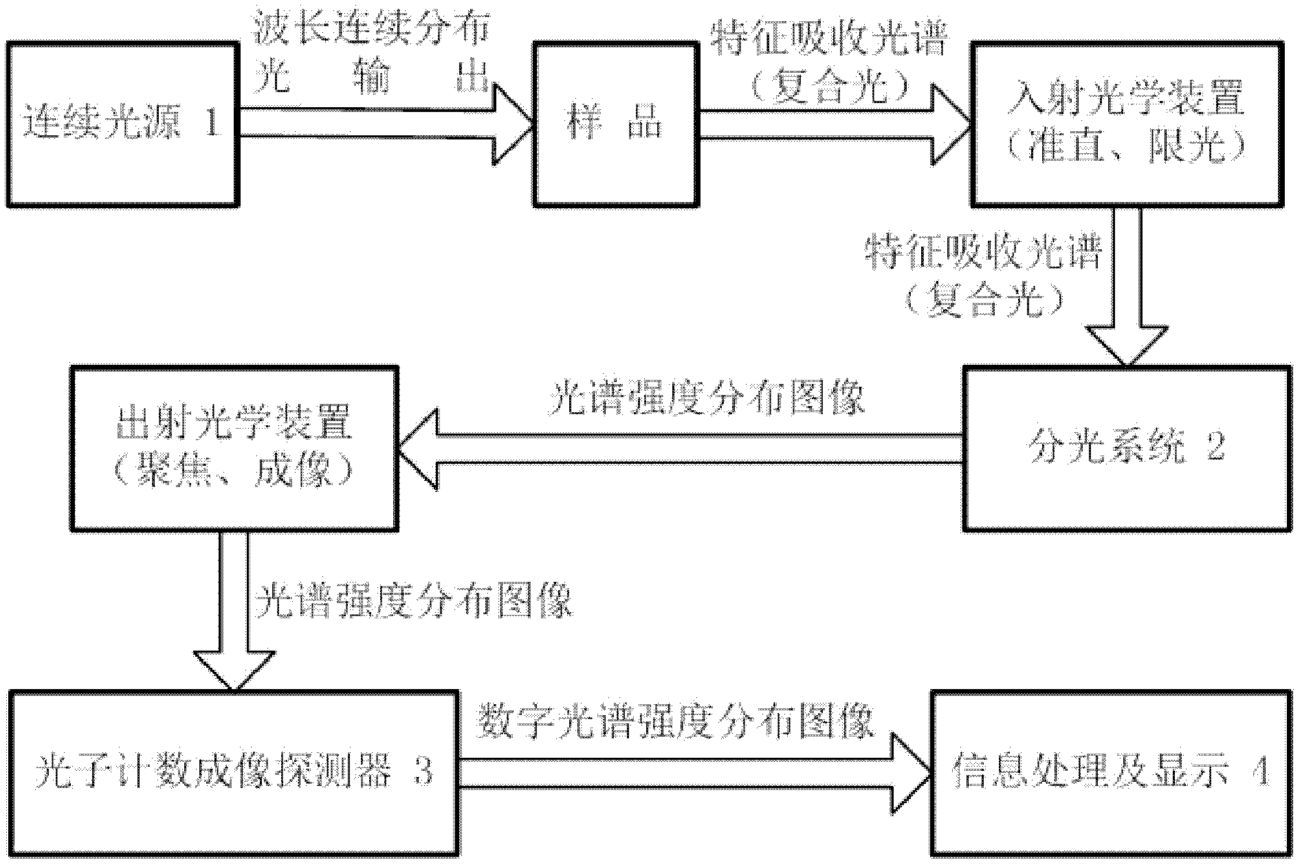
[0065] like figure 1 As shown, a photon counting full-spectrum direct-reading absorption spectrometer is mainly composed of a continuous light source 1, a spectroscopic system 2, a photon counting imaging detector 3, and information processing and display 4:
[0066] The continuous light source 1 is a light source device capable of providing light output with continuous wavelength distribution;
[0067] Spectroscopic system 2 is a dispersion spectroscopic device capable of dispersing composite light into monochromatic light or spectral intensity distribution images;
[0068] The photon counting imaging detector 3 is an image sensor capable of position-sensitive detection and photon counting;
[0069] Information processing and display 4 is used to receive and process optical images, and express the processing and analysis results in various graphic forms that are easy for people or machines to understand;
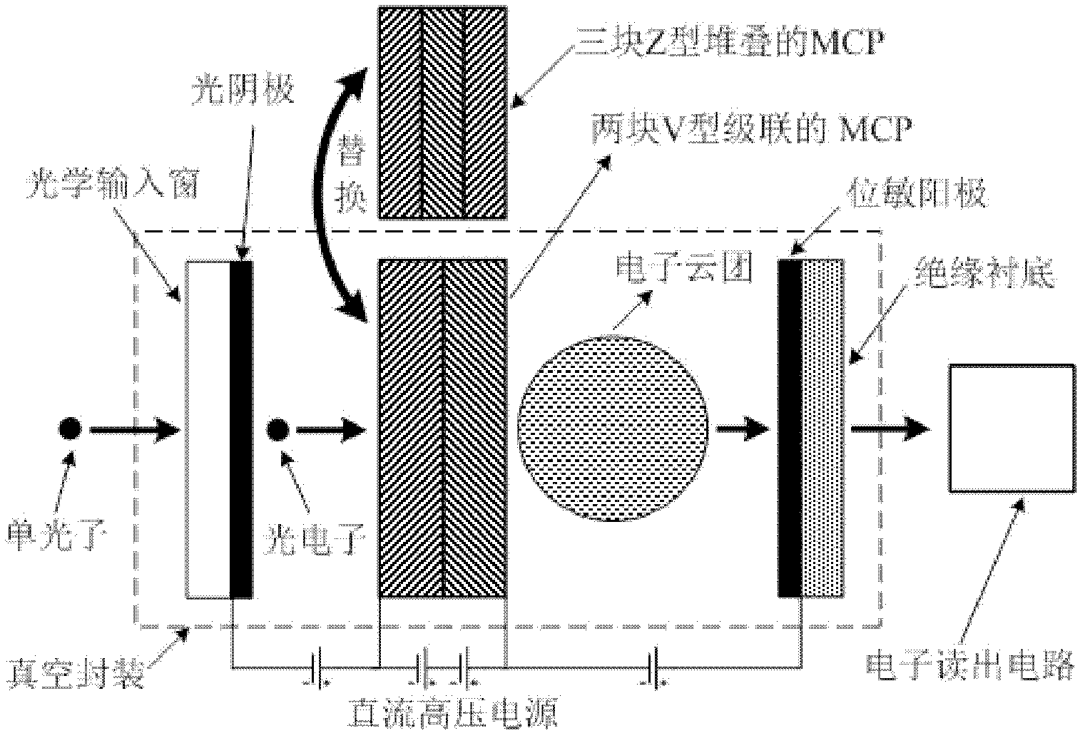
[0070] The optical connections between the continuous light source 1...
Embodiment 2
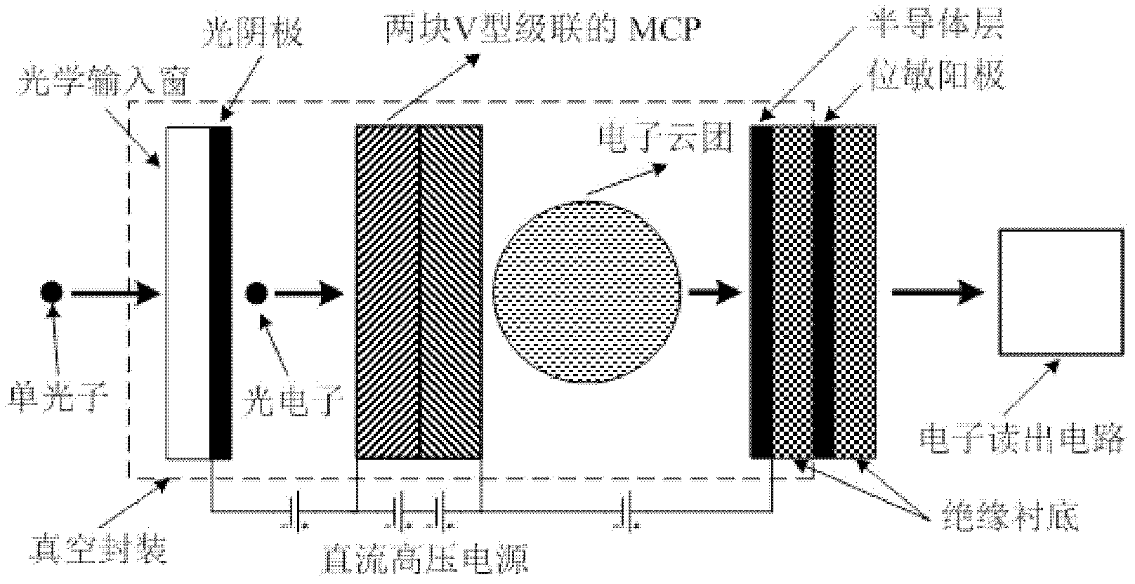
[0088] This embodiment is basically the same as Embodiment 1, the difference is that: on the basis of the photon counting imaging detector 3 described in Embodiment 1, a semiconductor layer can be added between the MCP output terminal and the position-sensitive anode, and the MCP There is a gap between the output terminal and the semiconductor layer, the semiconductor layer is plated on the insulating substrate, and the DC high-voltage power supply is electrically connected to the semiconductor layer through high-voltage leads or conductive electrodes (such as image 3 shown). At this time, the above step S540, that is, the physical process of collecting the electron cloud by the position-sensitive anode, evolves into: the electron cloud first crosses to the semiconductor layer under the action of the accelerating bias electric field, and then is induced to the position-sensitive anode through charge induction.
Embodiment 3
[0090]This embodiment is basically the same as Embodiment 1, except that: on the basis of the absorption spectrometer described in Embodiment 1, the light wavelength range output by the continuous light source 1 can be either a single ultraviolet or visible light band, or an ultraviolet -Composite bands such as visible light, visible light-near infrared and ultraviolet-near infrared. This example illustrates that the present invention can be used for absorption spectroscopy analysis in a variety of different wavelength ranges or bands.
PUM
 Abstract
Description
Claims
Application Information


