Tungsten diselenide and metal vertical schottky junction self-driven photoelectric detector and preparation

A photodetector, tungsten diselenide technology, applied in photovoltaic power generation, circuits, electrical components and other directions, can solve the problems of increased device cost, complex doping process, long response time, etc., to suppress reverse current, expand effective Lighting area, effect of suppressing increase

Active Publication Date: 2018-07-13
UNIV OF SCI & TECH BEIJING
View PDF3 Cites 4 Cited by
  • Summary
  • Abstract
  • Description
  • Claims
  • Application Information

AI Technical Summary

Problems solved by technology

Although junction detectors can solve the problems of long response time and external power supply, homogeneous PN junction photodetectors require complex doping processes, and heterogeneous PN junctions require multiple materials to be combined, increasing device costs

Method used


Image

  • Tungsten diselenide and metal vertical schottky junction self-driven photoelectric detector and preparation
  • Tungsten diselenide and metal vertical schottky junction self-driven photoelectric detector and preparation

Examples


Embodiment 1

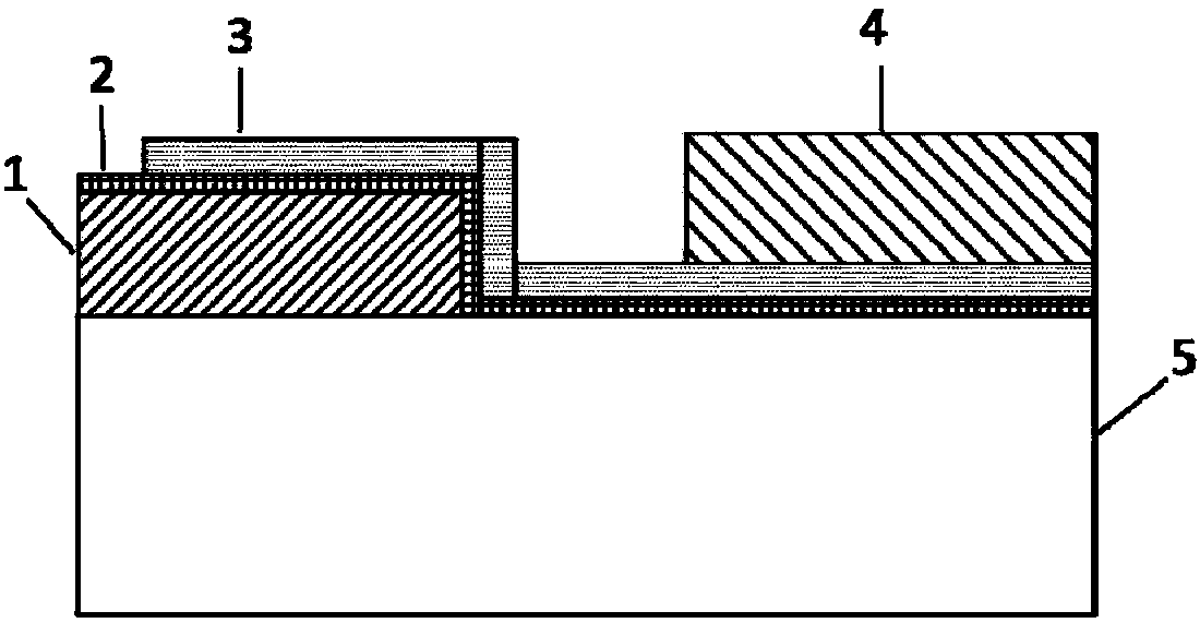
[0045] Tungsten diselenide and metal vertical Schottky junction self-driven photodetector, including source aluminum electrode, tunneling layer Al2O3, mechanically exfoliated 3nm thick tungsten diselenide, drain palladium electrode, insulating substrate silica. The aluminum electrode has a thickness of 20 nanometers; the aluminum oxide has a thickness of 0.5 nanometers; and the palladium electrode has a thickness of 30 nanometers. The specific preparation steps of the photodetector are as follows: first, put the insulating substrate silicon dioxide into three solutions of acetone, ethanol, and deionized water for 15 minutes, take it out, and dry it with nitrogen; then, use thermal evaporation or electron The aluminum electrode was evaporated on the silicon dioxide by beam evaporation; then, the tunneling layer aluminum oxide was deposited on the aluminum electrode by atomic layer deposition technology; again, the tungsten diselenide was transferred to the tunneling layer; fina...

Embodiment 2

[0047]Tungsten diselenide and metal vertical Schottky junction self-driven photodetector, including source aluminum electrode, tunneling layer Al2O3, mechanically exfoliated 1 nm thick tungsten diselenide, drain palladium electrode, insulating substrate silica. The titanium electrode has a thickness of 20 nanometers; the aluminum oxide has a thickness of 0.3 nanometers; and the palladium electrode has a thickness of 50 nanometers. The specific preparation steps of the photodetector are as follows: first, put the insulating substrate silicon dioxide into three solutions of acetone, ethanol, and deionized water for 15 minutes, take it out, and dry it with nitrogen; then, use thermal evaporation or electron The titanium electrode was evaporated on the silicon dioxide by beam evaporation; then, the tunneling layer aluminum oxide was deposited on the titanium electrode by atomic layer deposition technology; again, the tungsten diselenide was transferred to the tunneling layer; fina...


PUM

PropertyMeasurementUnit
thicknessaaaaaaaaaa
thicknessaaaaaaaaaa
thicknessaaaaaaaaaa

Abstract

The invention discloses a tungsten diselenide and metal vertical schottky junction self-driven photoelectric detector and preparation and belongs to the technical field of material application. The tungsten diselenide and metal vertical schottky junction self-driven photoelectric detector comprises an insulating substrate, a tunneling layer, a metal electrode and a tungsten diselenide nanosheet. Self-driven detection of a device is achieved by using a photovoltaic effect generated by a schottky junction formed by tungsten diselenide and metal under illumination, the light accepting area of a junction area is expanded through a vertical structure, an adjustable detection wavelength range is achieved through controlling the number of tungsten diselenide layers, increase of reverse current isinhibited through the tunneling layer, the sensitivity of the detector is improved and the response time is prolonged.

Description

technical field [0001] The invention belongs to the technical field of material application, in particular to a self-driven photodetector of tungsten diselenide and metal vertical Schottky junction and its preparation. Background technique [0002] In 2011, B.Radisavljevic and others discovered that transition metal chalcogenides represented by single-layer molybdenum disulfide are different from the zero band gap of graphene. This type of layered material has very superior optical, electrical, magnetic and other physical properties. Chemical properties, which have received extensive attention in the fields of electronics and optoelectronics, are considered candidates for the development of next-generation nano-optoelectronic devices. Tungsten diselenide is a typical bipolar two-dimensional semiconductor, and the layers are connected by van der Waals bonds; the band gap can be changed from the indirect band gap of the multilayer (1.3 electron volts) to the direct band gap of...

Claims


Application Information

Patent Timeline
Patent Type & Authority Applications(China)
IPC IPC(8): H01L31/032H01L31/0352H01L31/108H01L31/18B82Y30/00B82Y40/00
CPCB82Y30/00B82Y40/00H01L31/032H01L31/03529H01L31/108H01L31/18Y02E10/50Y02P70/50
Inventor 张跃杜君莉张铮柳柏杉张先坤王可汗于慧慧高丽
Owner UNIV OF SCI & TECH BEIJING
Why Eureka
Try Eureka