Large-scale controllable preparation method of surface plasmon nanonail structure

A technology of surface plasmons and nano-nails, applied in separation methods, nanotechnology for materials and surface science, chemical instruments and methods, etc., can solve problems such as narrow-spectrum resonance effects, reduce production costs, and achieve realization shape-controllable effect

Inactive Publication Date: 2018-08-03
SOUTHEAST UNIV
View PDF0 Cites 5 Cited by
  • Summary
  • Abstract
  • Description
  • Claims
  • Application Information

AI Technical Summary

Problems solved by technology

[0005] Technical problem: The purpose of the present invention is to overcome the deficiencies of the prior art, and propose a method for the large-scale controllable preparation of a surface plasmon nanonail structure. The chemical method has simple synthesis steps, good repeatability, and is easy to Industrialized mass production, and compared with the expensive top-down process, the production cost can be significantly reduced; the shape and size of the prepared surface plasmon nanonail photoelectric material can be precisely controlled, and the decahedral core can be controlled by controlling the The diameter is used to control the thickness of the growing nanorods, and the surface plasmon nanonails formed by growing silver triangular plates on the surface defects of the nanorods have narrower spectra and stronger resonance effects in the visible to near-infrared bands. , nano-integrated optical devices and nano-optical materials have broad application prospects

Method used


Image

  • Large-scale controllable preparation method of surface plasmon nanonail structure
  • Large-scale controllable preparation method of surface plasmon nanonail structure
  • Large-scale controllable preparation method of surface plasmon nanonail structure

Examples


Embodiment 1

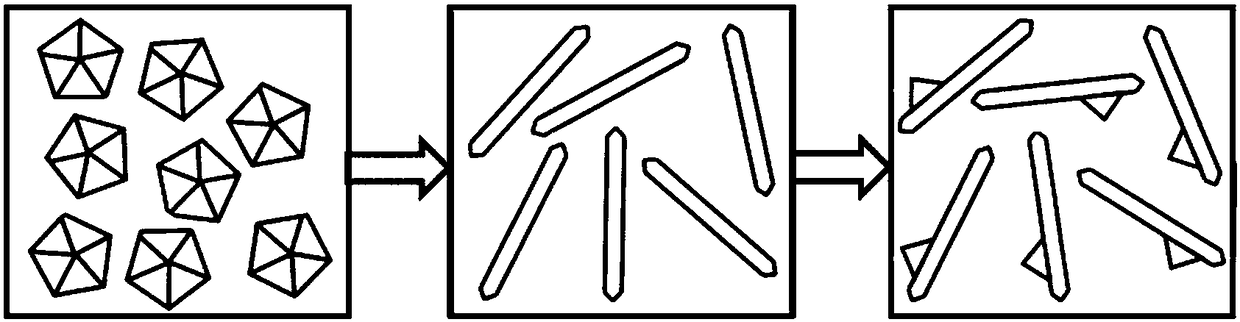
[0069] 1. Synthesis of silver nanonails whose backbone is silver nanorods:

[0070] (1) Illumination-induced growth of decahedral nuclei

[0071] Add 0.52ml 0.5M sodium citrate, 15ul 0.5M PVP (molecular weight 40k), 0.05ml 0.05M L-arginine and 0.4ml 0.05M silver nitrate to 150ml water, stir for 5min and then add 2ml 0.1M Sodium borohydride, continue to stir for 45 minutes, add a small amount of hydrogen peroxide solution, stir for 25 minutes, and irradiate the mixed solution with light for 2 hours to obtain a silver decahedron solution.

[0072] (2) Chemical reduction growth of silver nanorods

[0073] Add 0.72ml 0.5M sodium citrate and 0.135ml 0.5M PVP to 60ml water, heat and stir at 115°C for 10min, add 0.4ml 0.05M silver nitrate, and add the silver decahedron prepared in step (1) at the same time, stop heating after 10min , to obtain a silver nanorod solution.

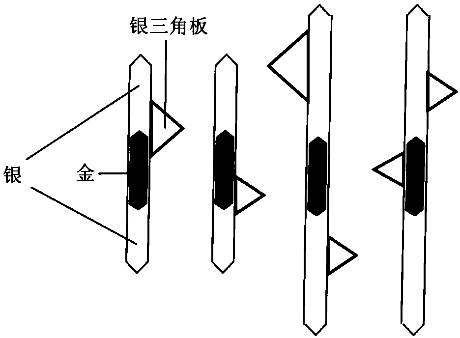
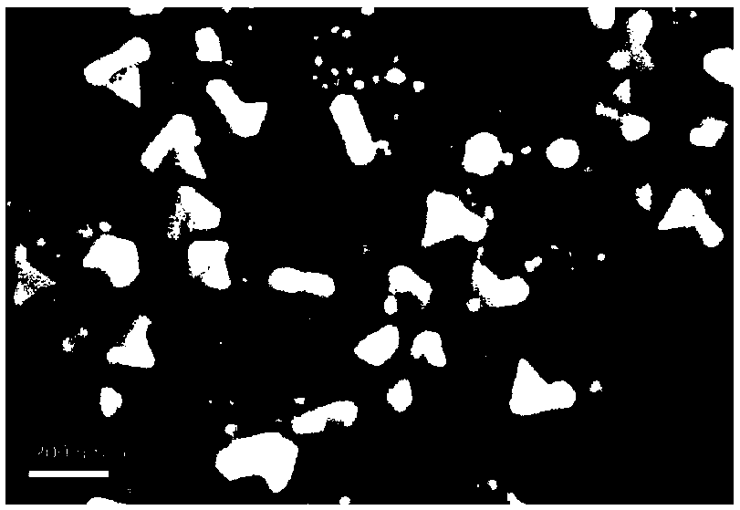
[0074] (3) Ingot epitaxial growth into nano-nails

[0075] Centrifuge the nanorod solution prepared in step (...


PUM

PropertyMeasurementUnit
molecular weightaaaaaaaaaa
q valueaaaaaaaaaa

Abstract

The invention provides a large-scale controllable preparation method of a surface plasmon nanonail photoelectric structure. The size of the nanometer material can be controlled at sub-wavelength. Thenanometer material has good localized surface plasmon resonance effect, and the optical, electrical and mechanical properties of the nanometer material all can be regulated and controlled. The surfaceplasmon nanonail is composed of two parts including a silver nanorod or a silver-gold-silver alloy nanorod and an approximate equilateral triangular nano-silver sheet growing on the nanorod. The length of the nanorod is controlled within 20-30 nanometers, the diameter of the nanorod is controlled within 10-200 nanometers, the side length of the triangular nano-silver sheet is controlled within 20nannometers to 2 microns, and the size of the triangular sheet is less than or equal to the length of the nanorod. The plasmon nanonail photoelectric structure has the characteristics of the tunablespectrum, the narrow-band resonance enhancement effect, high Q value and the like. Accordingly, the silver nanonail has extensive application prospects.

Description

technical field [0001] The invention relates to the fields of crystal growth, nano-integrated optical devices and nano-photoelectric materials, in particular to a controllable preparation method of surface plasmon nano-nail photoelectric materials. Background technique [0002] With the continuous deepening of research on nanomaterials, basic units such as zero-dimensional quantum dots, one-dimensional nanowires and nanorods, two-dimensional nanoplates, and three-dimensional nanotubes have relatively mature preparation methods. Such nanomaterials have been widely used in many fields such as optoelectronic materials, chemical biosensing, and catalysis. However, the performance of single-structure nanomaterials has great limitations. In this era of continuous development of science and technology, the demand for more novel and better-performing nanomaterials and nanodevices continues to increase. The preparation of complex and diverse nanomaterials has become It has become an...

Claims


Application Information

Patent Timeline
Patent Type & Authority Applications(China)
IPC IPC(8): B22F9/24B22F1/00B82Y40/00B22F1/062B22F1/145B22F1/17
CPCB82Y40/00B22F9/24B22F1/07B22F1/145B22F1/062B22F1/17B22F2999/00C22C1/0466B82Y20/00B01D57/02B22F2301/255B82Y30/00
Inventor 张晓阳张彤薛小枚秦妍妍
Owner SOUTHEAST UNIV
Why Eureka
Try Eureka