Semiconductor diode chip and manufacturing method thereof

A diode and semiconductor technology, applied in the field of diode chips, semiconductor diode chips and their production, can solve the problems of large trench occupation area, easy discharge and ignition, short service life, etc., and achieve large effective use area and good high temperature reliability , the effect of strong pressure resistance

Inactive Publication Date: 2018-08-03
济南兰星电子有限公司
View PDF12 Cites 8 Cited by
  • Summary
  • Abstract
  • Description
  • Claims
  • Application Information

AI Technical Summary

Problems solved by technology

At present, there are many processes for making GPP diodes in the diode industry. For example, the current mainstream processes include knife-scratch GPP process, photoresist GPP process, electrophoresis GPP process, GPRC process, PIPP process, etc. Among them, knife-scratch GPP process, photoresist GPP process, Electrophoretic GPP process products almost occupy more than 90% of the diode market, and these three main processes have some shortcomings, for example, 1. The sharp corners of the countertops of the GPP process products (commonly known as "bird's beak", this article is called "bird's beak") mouth") without glass protection, the test is easy to discharge and ignite, the high temperature leakage is large, and the high temperature stability is poor; In particular, the chip on the edge of the silicon wafer is more likely to be damaged during the production process, and the groove occupies a large area. Compared with other processes with the same chip size, the effective welding area is small and the VF is high; 3. Electrophoresis GPP process products The passivation glass is thinner, which leads to the disadvantages of low voltage withstand capability and short service life of the device

Method used


Image

  • Semiconductor diode chip and manufacturing method thereof
  • Semiconductor diode chip and manufacturing method thereof

Examples


Embodiment 1

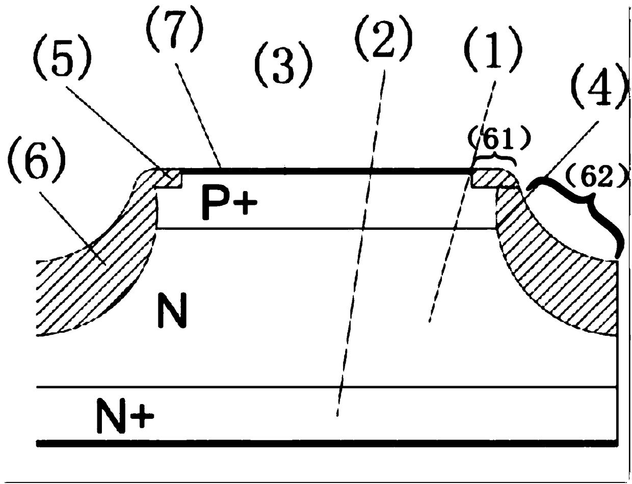
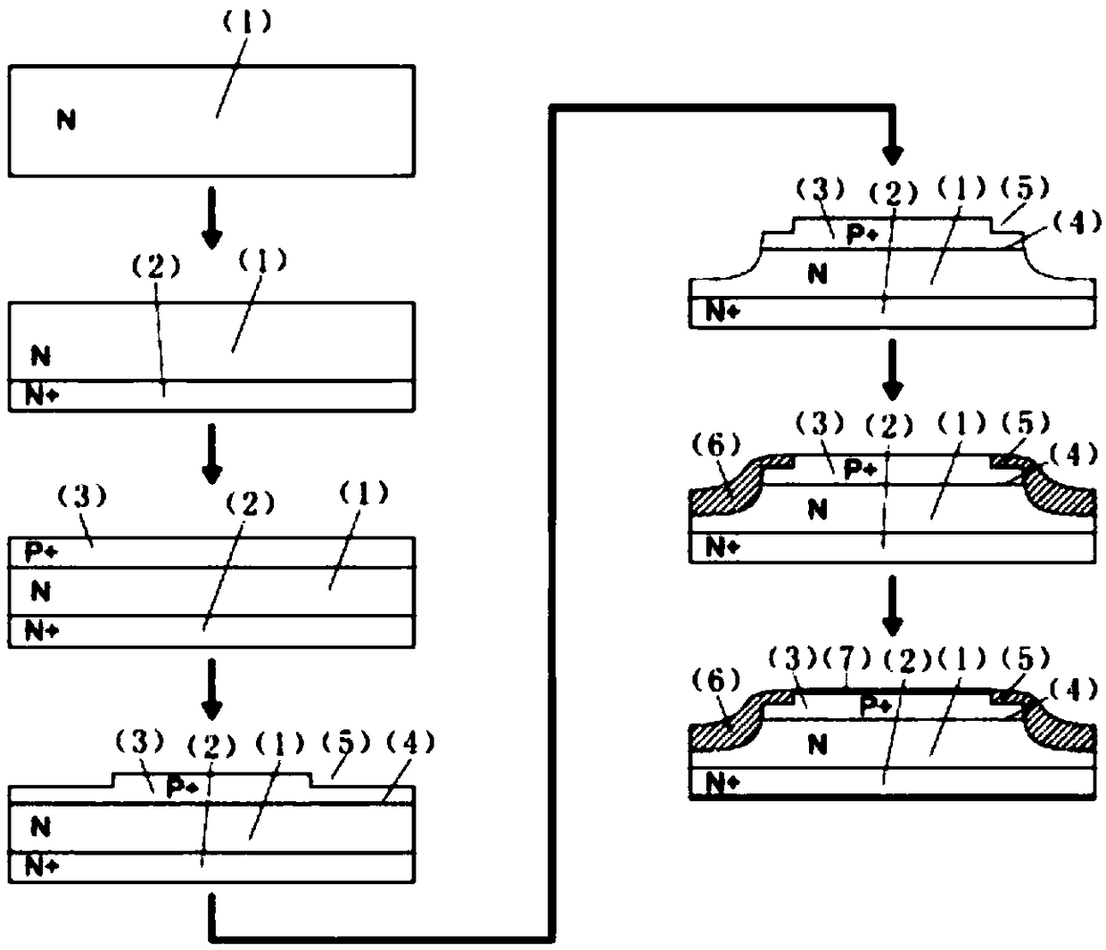
[0036] Example 1, such as figure 1 Shown, the present invention provides a kind of semiconductor diode chip, comprises silicon chip substrate, and the bottom of its silicon chip substrate is provided with phosphorus diffusion layer, and upper part is provided with boron diffusion layer, for the shape of silicon chip substrate and boron diffusion layer The design is also relatively simple, mainly depending on the design of the external passivation layer. In addition, the upper part of the boron diffusion layer and the bottom of the phosphorus diffusion layer are provided with metal electrodes. For welding, the inventor is provided with a novel passivation layer wrapping the silicon wafer substrate and the side of the boron diffusion layer on the outside of the silicon wafer substrate (chip), from figure 1 It can be seen from the figure that the new passivation layer includes the silicon wafer substrate and the surrounding sides of the boron diffusion layer. However, when the ne...


PUM


Abstract

The invention belongs to the technical field of semiconductors, and relates to a diode chip, in particular to a semiconductor diode chip and a manufacturing method thereof. The semiconductor diode chip comprises a silicon chip substrate, wherein the bottom part of the silicon chip substrate is provided with a phosphorus diffusion layer, the upper part is provided with a boron diffusion layer, metal electrodes are arranged on the upper part of the boron diffusion layer and the bottom part of the phosphorus diffusion layer, a novel passivation layer is arranged at the outer side of the peripheryof the silicon chip substrate, and the novel passivation layer comprises a transition portion and a 'beak' portion. The manufacturing method comprises the steps of original sheet cleaning, diffusion,sand blasting, cleaning, primary photoetching, stepped corrosion, secondary photoetching, grooving corrosion, cleaning, passivation, third-time photoetching, metallization, electrical performance testing and scribing. The semiconductor diode chip has the advantages that the 'beak' portion of the semiconductor diode chip is protected by glass, the glass is not higher than the table board of the chip, ignition is not caused, the manufacturing cost is low (higher than that of a knife scraping manufacturing process, and lower than that of a photoresist manufacturing process), the effective use area of the chip is large, the VF is lower, the glass is thick, the pressure endurance capability is high, the service life is long, the high temperature reliability is high and the like.

Description

technical field [0001] The invention belongs to the technical field of semiconductors and relates to diode chips, in particular to a semiconductor diode chip and a manufacturing method thereof. Background technique [0002] With the advancement and development of semiconductor technology, the performance requirements of semiconductor devices are getting higher and higher. In the diode industry, the improvement of device performance is undoubtedly due to the birth of the GPP process. The so-called GPP process is the use of glass to passivate the surface of the PN junction. The process, the device produced by this process has high electrical performance and reliability, and the passivation material glass has good chemical stability. This process mainly exposes the PN junction through trench corrosion, and then cleans the PN junction surface to obtain a clean PN junction surface, then directly coats the glass on the PN junction surface, and melts it according to the temperature...

Claims


Application Information

Patent Timeline
Patent Type & Authority Applications(China)
IPC IPC(8): H01L29/861H01L23/31H01L21/329H01L21/56
CPCH01L21/56H01L23/3171H01L23/3185H01L29/6609H01L29/8613
Inventor 魏兴政李浩
Owner 济南兰星电子有限公司
Why Eureka
Try Eureka