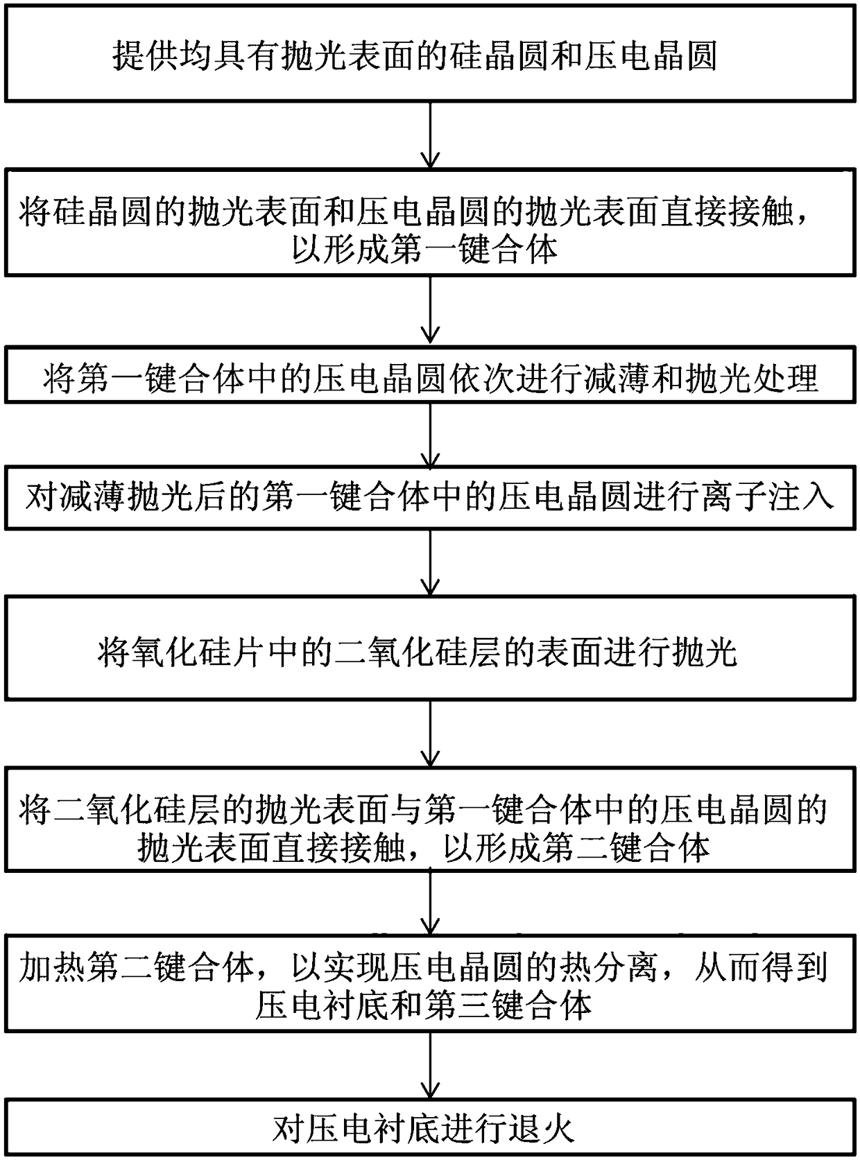
Manufacturing method of composite piezoelectric substrate for surface acoustic wave device
A technology of surface acoustic wave devices and manufacturing methods, applied in semiconductor/solid-state device manufacturing, piezoelectric devices/electrostrictive devices, device components, etc., can solve the problems of increased production process risks and costs, fragmentation, and low cooling efficiency To achieve the effect of reducing process risk and process cost, improving material utilization rate and shortening production cycle
- Summary
- Abstract
- Description
- Claims
- Application Information
AI Technical Summary
Problems solved by technology
Method used
Image
Examples
Embodiment 1
[0059] (1) Provide a 3-inch Z-cut lithium tantalate wafer, provide a 3-inch monocrystalline silicon wafer, place the lithium tantalate wafer and silicon wafer on the porous ceramic suction cup of the polishing machine, and adjust the inclination of the spindle , to polish the surface to obtain a smooth surface. The polished wafer is cleaned at the semiconductor level to obtain a wafer with a clean surface.
[0060] (2) The wafer with a clean surface obtained in step (1) is directly contacted at room temperature, and the lithium tantalate wafer and the silicon wafer are bonded together due to the van der Waals force.
[0061] (3) Thinning the lithium tantalate wafer in the above bonding body to 20um, and then performing chemical mechanical polishing to obtain a smooth surface.
[0062] (4) Perform He on the lithium tantalate wafer surface of the bonding body + Ion implantation determines the depth of the implanted layer by controlling the implantation energy. The injected do...
Embodiment 2
[0066] (1) Provide a 3-inch Z-cut lithium niobate wafer and a 3-inch silicon wafer, respectively place one wafer surface of the lithium niobate and silicon wafer on the porous ceramic suction cup of the polishing machine, and adjust the inclination of the spindle , to polish the surface to obtain a smooth surface. The polished wafer is subjected to semiconductor-grade cleaning to obtain a wafer with a clean surface.
[0067] (2) The wafer with a clean surface obtained in step (1) is directly contacted at room temperature, and the lithium niobate wafer and the silicon wafer are bonded together due to the van der Waals force.
[0068] (3) Thinning the lithium niobate wafer in the above bonding body to 30um, and then performing chemical mechanical polishing to obtain a smooth surface.
[0069] (4) The lithium niobate wafer surface of the bonding body is implanted with He by ion implantation + , by controlling the implant energy to determine the depth of the implanted layer. Th...
PUM
 Abstract
Description
Claims
Application Information


