Wavefront scanning modulator based on high electron mobility transistor

A technology with high electron mobility and fast scanning, applied in the direction of electric solid-state devices, semiconductor devices, circuits, etc., can solve the problem that the spatial light modulator technology cannot be directly applied to the terahertz band, achieve good practical application prospects, and avoid high difficulty The effect of processing and mature technology

Inactive Publication Date: 2018-08-17
UNIV OF ELECTRONICS SCI & TECH OF CHINA
View PDF8 Cites 0 Cited by
  • Summary
  • Abstract
  • Description
  • Claims
  • Application Information

AI Technical Summary

Problems solved by technology

However, due to the lack of materials that respond to terahertz and the mismatch between material structure parameters and terahertz wavelengths, the traditional spatial light modulator technology cannot be directly applied to the terahertz band.

Method used


Image

  • Wavefront scanning modulator based on high electron mobility transistor
  • Wavefront scanning modulator based on high electron mobility transistor
  • Wavefront scanning modulator based on high electron mobility transistor

Examples


Embodiment Construction

[0027] The present invention will be further described below in conjunction with the accompanying drawings and embodiments.

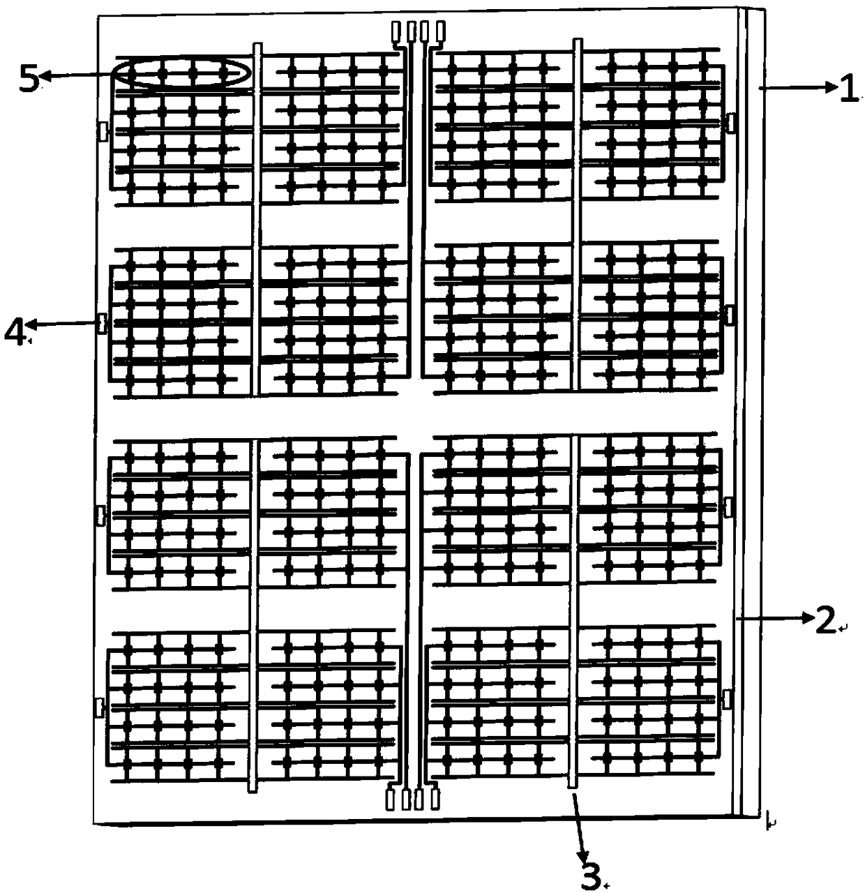
[0028] This embodiment provides a wavefront rapid scanning imaging modulator based on high electron mobility transistors, its structure diagram is as follows figure 1 As shown, it includes semiconductor 1, epitaxial layer 2, positive voltage loading pole 3, negative voltage loading pole 4 and 4*4 pixel units 5; epitaxial layer 2 is located on the upper surface of semiconductor substrate 1, positive voltage loading pole 3, negative voltage loading pole 4 The voltage loading electrode 4 and the pixel unit 5 are located on the upper surface of the epitaxial layer 2;

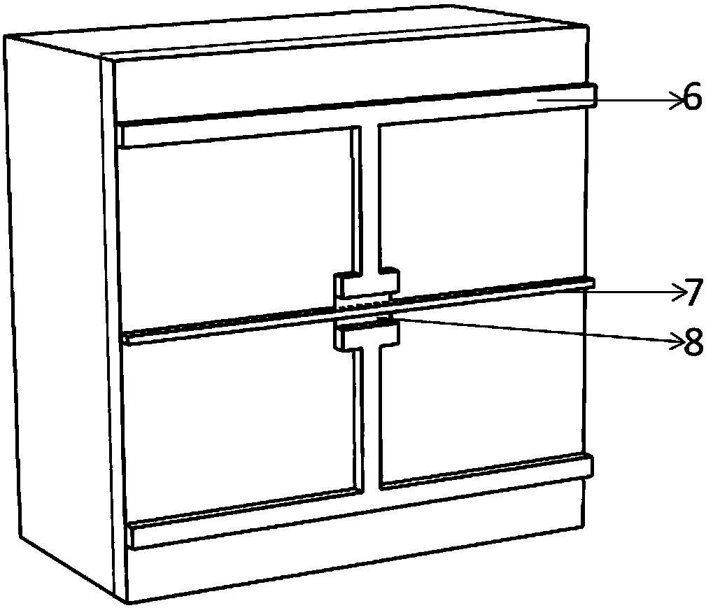
[0029] Each pixel unit 5 includes 4*4 subunits, and the structural diagram of the subunits is as follows image 3 As shown, each subunit includes a metal I-shaped artificial microstructure 6, a gate connection line 7 and a semiconductor-doped heterostructure 8; there is an opening in the mid...


PUM


Abstract

The invention discloses a multi-pixel wavefront scanning modulator based on a high electron mobility transistor (HEMT), belongs to the technical field of electromagnetic functional devices. Accordingto the invention, the HEMT and the artificial electromagnetic medium resonance structure are combined, and a multi-pixel structure system is formed through multi-unit combination. Rapid multi-pixel modulation of the wavefront can be realized. External voltage is used for independently controlling the pixel units of the wave-front modulator, and the concentration of the two-dimensional electron gasin an HEMT epitaxial layer is controlled through the loaded voltage signals, and therefore the electromagnetic resonance mode of the artificial electromagnetic medium resonance structure is changed.Rapid modulation of the wavefront can be realized. The multi-pixel wavefront scanning modulator can be used for a wavefront rapid scanning imaging system, and has a high amplitude modulation depth ata working frequency point. The simulation result can reach 90%. The multi-pixel wavefront scanning modulator is simple in structure, easy to machine, high in modulation speed, convenient to use and easy to pack.

Description

technical field [0001] The invention belongs to the technical field of electromagnetic functional devices, and in particular relates to a high-electron-mobility transistor-based wavefront rapid scanning imaging modulator. Background technique [0002] In recent years, with the development of semiconductor materials and technologies, high electron mobility transistors (High Electron Mobility Transistor, HEMT) have shown outstanding advantages. At present, the development prospects of HEMT devices are very promising. Due to their low noise, low power consumption, and ultra-high speed, they have been widely used in satellite communications, ultra-high-speed computers, and signal processing. . A high electron mobility transistor (High Electron Mobility Transistor, HEMT) is a new type of field effect transistor that utilizes the two-dimensional electron gas (2-DEG) existing in the modulated doped heterojunction to work. HEMT has experienced 37 years of development since it was ...

Claims


Application Information

Patent Timeline
Patent Type & Authority Applications(China)
IPC IPC(8): H01L27/146H04L27/04
CPCH01L27/14601H01L27/14609H04L27/04
Inventor 张雅鑫蔡雪丹张亭曾泓鑫梁士雄杨梓强
Owner UNIV OF ELECTRONICS SCI & TECH OF CHINA
Why Eureka
Try Eureka