
A Dielectric Integrated Waveguide Filter Based on Gallium Arsenide Technology

A filter and dielectric substrate technology, applied in waveguide-type devices, circuits, electrical components, etc., can solve the problems of increased manufacturing cost, large physical size, electromagnetic energy leakage, etc., to achieve easy processing, compact structure, high frequency selection sexual effect

Active Publication Date: 2020-03-17
BEIJING INSTITUTE OF TECHNOLOGYGY
View PDF6 Cites 0 Cited by
  • Summary
  • Abstract
  • Description
  • Claims
  • Application Information

AI Technical Summary

Problems solved by technology

When metal waveguide filters are applied to miniaturized transceiver components, there are two significant problems: first, the physical size is relatively large, occupying a large area in the transceiver components, which is not conducive to the miniaturization design of TR components, while filtering The device needs to be split into two halves to be processed on the cavity and the cover respectively, which increases the manufacturing cost and introduces assembly errors; second, an additional waveguide-microstrip transition structure is required to interconnect with other components in the component, and the transmission and reception components The available space is further squeezed, which also increases the complexity of the components
[0008] Literature Wu Y Q, Xu P P.Cross-coupled substrate integrated waveguide filter with sharp sideband performance[C].International Workshop on Microwave andMillimeter Wave Circuits and System Technology(IEEE,2014:272-274) introduced a folding SIW belt Pass filter, which utilizes the folded form of the structure to realize the negative cross-coupling between non-adjacent resonators, thus generating a transmission zero at the low end of the filter passband, but the filter based on this topology The device is large in size and complex in processing
Literature Wong S W, Wang K, Chen Z N, et al. Electric Coupling Structure of Substrate Integrated Waveguide (SIW) for the Application of 140-GHz BandpassFilter on LTCC [J]. IEEE Transactions on Components Packaging & Manufacturing Technology (2014,4(2):316 -322) introduced a SIW bandpass filter composed of cascaded electromagnetic bandgap (EBG). Energy leakage, and reduces the Q value of the resonator, which has a certain degree of impact on the performance of the filter

Method used


Image

  • A Dielectric Integrated Waveguide Filter Based on Gallium Arsenide Technology
  • A Dielectric Integrated Waveguide Filter Based on Gallium Arsenide Technology
  • A Dielectric Integrated Waveguide Filter Based on Gallium Arsenide Technology

Examples


Embodiment Construction

[0037] The present invention will be described in detail below with reference to the accompanying drawings and examples.

[0038] Group III-V compound semiconductor materials represented by gallium arsenide (GaAs) have the characteristics of high electron mobility, high temperature resistance, radiation resistance, and easy growth of heterostructures. Semiconductor devices based on this substrate have the characteristics of high operating frequency, stable high and low temperature performance, and low noise, so they have been widely used in the design of W-band active devices. At the same time, because the GaAs process has the characteristics of high precision, if the GaAs process is used to develop the SIW filter, the problem of insufficient precision in the W-band of the traditional circuit integration process can be solved, but there are few work reports in this area at present.

[0039] Therefore, the present invention proposes a GaAs technology-based dielectric integrated...


PUM


Abstract

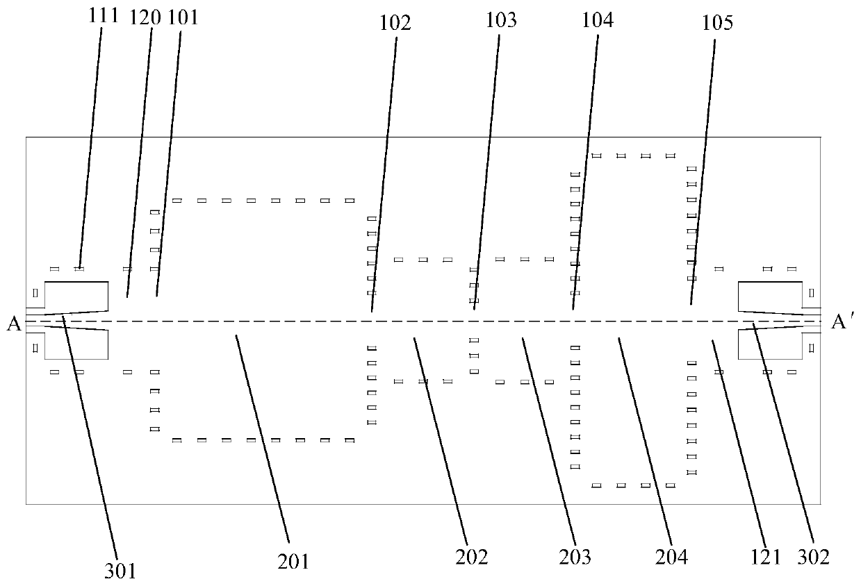
The invention discloses a dielectric integrated waveguide filter based on the gallium arsenide technology, and is developed on the basis of a multi-mode resonant cavity, and electromagnetic waves cangenerate electromagnetic cancellation in the multi-mode resonant cavity through reasonable design of the size of the multi-mode resonant cavity, so that a transmission zero point can be generated. Byadopting the technical means of changing the length-width ratio of the cavity, the position of the transmission zero point can be controlled, transmission zero points can be respectively designed at the low end and the high end of the filter near the pass band, so that the filter has high-frequency selectivity; the filter is developed by a 70-micron gallium arsenide technology, and both ends of the filter are GSG structures, the filter chip can be integrated with other W-waveband active chips based on the 70-micron gallium arsenide technology, and not only the chip-chip direct interconnectionmode is adopted, and the filter and other chips can be directly integrated on the same chip.

Description

technical field [0001] The invention belongs to the technical field of millimeter wave filters, and in particular relates to a dielectric integrated waveguide filter based on gallium arsenide technology. Background technique [0002] In radar, communication and other electronic equipment, the filter is one of the indispensable key components in the radio frequency transceiver circuit (component). Since the physical size of the filter is usually several times the working wavelength, the miniaturization and planar design of the filter determine the overall miniaturization and integration of the transceiver components. In the microwave frequency band, commonly used filters can be divided into microstrip and waveguide forms. However, as the frequency increases, the Q value of the microstrip filter decreases and the selectivity becomes poor, which cannot meet the application requirements in the W-band. When the system requires the filter to have both low insertion loss and high...

Claims


Application Information

Patent Timeline
Patent Type & Authority Patents(China)
IPC IPC(8): H01P1/20H01P1/208
CPCH01P1/20H01P1/208
Inventor 肖钰单培哲朱凯强孙厚军
Owner BEIJING INSTITUTE OF TECHNOLOGYGY
Learn More