Light emitting diode epitaxial wafer and manufacturing method thereof

A technology of light-emitting diodes and manufacturing methods, applied to electrical components, circuits, semiconductor devices, etc., can solve the problems of many crystals, low growth temperature, and affecting the luminous efficiency of light-emitting diodes, so as to improve crystal quality, improve luminous efficiency, and reduce defects Effect

Active Publication Date: 2018-08-31
HC SEMITEK ZHEJIANG CO LTD
View PDF7 Cites 6 Cited by
  • Summary
  • Abstract
  • Description
  • Claims
  • Application Information

AI Technical Summary

Problems solved by technology

[0006] In order to solve the problem in the prior art that the growth temperature of the low-temperature P-type layer is low, the crystal produces more defects, and the luminous efficiency of the light-emitting diode is affected, the embodiment of the present invention provides a light-emitting diode epitaxial wafer and a manufacturing method thereof

Method used


Image

  • Light emitting diode epitaxial wafer and manufacturing method thereof
  • Light emitting diode epitaxial wafer and manufacturing method thereof

Examples


Embodiment 1

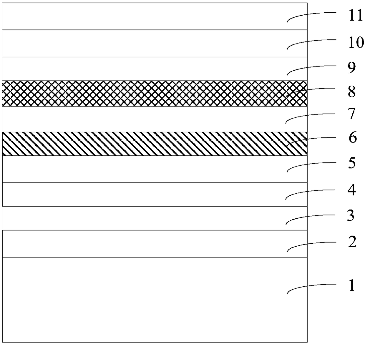
[0031] An embodiment of the present invention provides a light emitting diode, figure 1 It is a schematic structural diagram of a light-emitting diode epitaxial wafer provided by an embodiment of the present invention, as shown in figure 1 As shown, the light-emitting diode includes a substrate 1, and a low-temperature buffer layer 2, a high-temperature buffer layer 3, an N-type layer 4, an active layer 5, a first insertion layer 6, and a low-temperature P-type layer stacked on the substrate 1 in sequence. Layer 7, second insertion layer 8, electron blocking layer 9, high temperature P-type layer 10 and P-type contact layer 11. Wherein, the growth temperature of the low-temperature P-type layer 7 is 720-790°C.

[0032] The first insertion layer 6 is an Al-GaN / GaN superlattice structure with a period of n, 2≤n≤10, the growth temperature of the first insertion layer 6 is the same as that of the low-temperature P-type layer 7, and the second insertion layer 8 It is an Al-doped ...

Embodiment 2

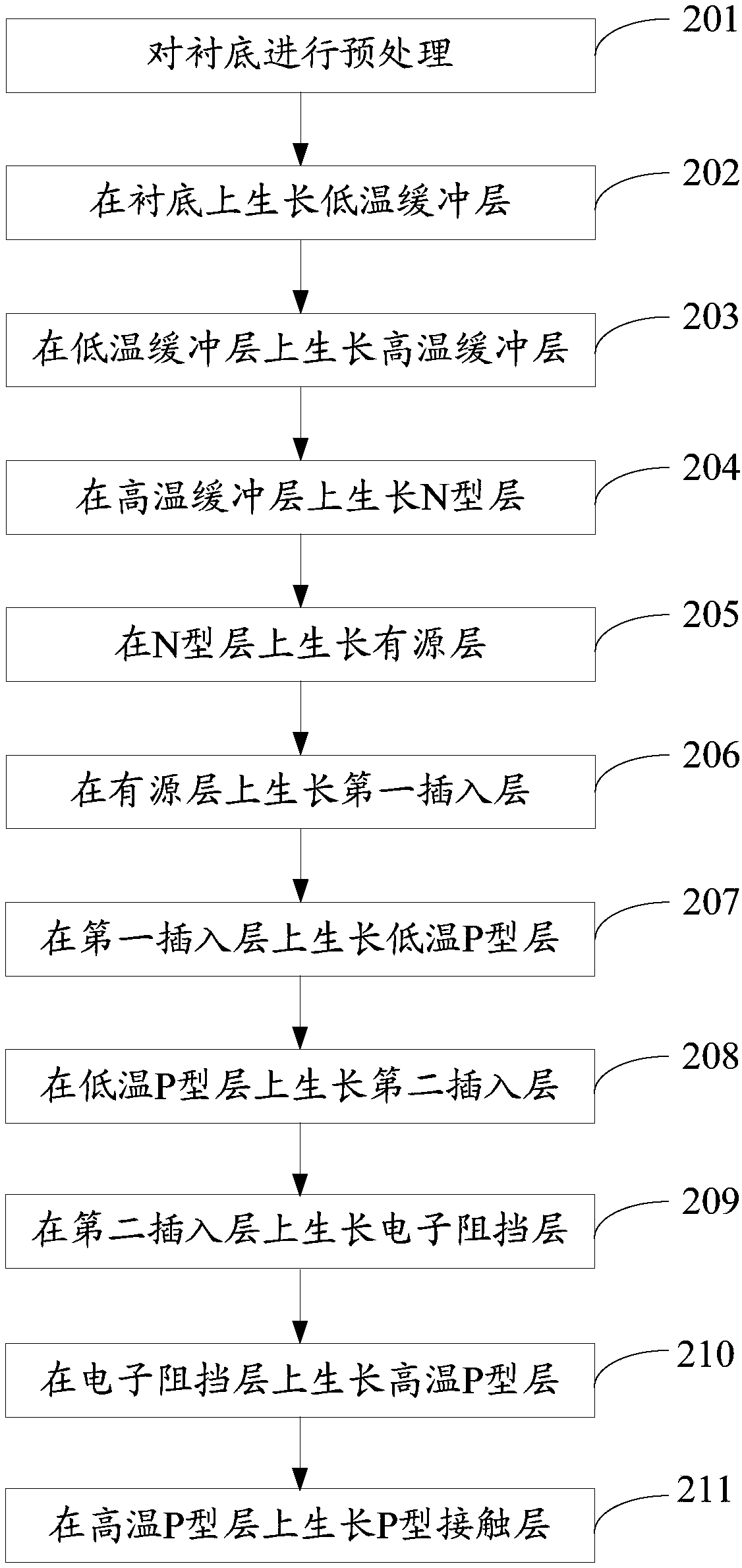
[0046] An embodiment of the present invention provides a method for manufacturing a light-emitting diode epitaxial wafer, which is suitable for the light-emitting diode epitaxial wafer provided in Embodiment 1. figure 2 It is a method flowchart of a method for manufacturing a light-emitting diode epitaxial wafer provided by an embodiment of the present invention, as shown in figure 2 As shown, the manufacturing method includes:

[0047] Step 201, performing pretreatment on the substrate.

[0048] Optionally, the substrate is sapphire with a thickness of 630-650um.

[0049] In this embodiment, Veeco K465i or C4MOCVD (Metal Organic Chemical VaporDeposition, metal organic compound chemical vapor deposition) equipment is used to realize the LED growth method. Using high-purity H 2 (hydrogen) or high-purity N 2 (nitrogen) or high purity H 2 and high purity N 2 The mixed gas as the carrier gas, high-purity NH 3 As the N source, trimethylgallium (TMGa) and triethylgallium (T...


PUM


Abstract

The invention discloses a light emitting diode epitaxial wafer and a manufacturing method thereof and belongs to the technical field of semiconductors. The light emitting diode epitaxial sheet comprises a substrate, a low-temperature buffering layer, a high-temperature buffering layer, an N-type layer, an active layer, a low-temperature P-type layer, an electronic blocking layer, a high-temperature P-type layer and a P-type contract layer, wherein the low-temperature buffering layer, the high-temperature buffering layer, the N-type layer, the active layer, the low-temperature P-type layer, theelectronic blocking layer, the high-temperature P-type layer and the P-type contract layer are successively laminated on the substrate. The growth temperature of the low-temperature P-type layer is 720-790 DEG C. A first insertion layer is arranged between the low-temperature P-type layer and the active layer. The first insertion layer is of an Al-GaN/GaN superlattice structure with the period ofn, wherein 2<=n<=10. The growth temperature of the first insertion layer is the same as that of the low-temperature P-type layer. A second insertion layer is arranged between the low-temperature P-type layer and the electronic blocking layer. The second insertion layer is of a GaN structure doped with Al. The growth temperature of the second insertion layer is 10-50 DEG C higher than the growth temperature of the low-temperature P-type layer. By setting the first insertion layer and the second insertion layer, production of defects is reduced and light emitting efficiency of the light emitting diode can be improved.

Description

technical field [0001] The invention relates to the technical field of semiconductors, in particular to a light-emitting diode epitaxial wafer and a manufacturing method thereof. Background technique [0002] LED (Light Emitting Diode, Light Emitting Diode) is a semiconductor electronic component that can emit light. As an efficient, environmentally friendly and green new solid-state lighting source, it is being rapidly and widely used, such as traffic lights, car interior and exterior lights, urban landscape lighting, mobile phone backlight, etc. Improving the luminous efficiency of chips is the goal that LEDs are constantly pursuing. [0003] The existing manufacturing method of LED epitaxial wafers includes: sequentially growing a low-temperature buffer layer, a high-temperature buffer layer, an N-type layer, an active layer, a low-temperature P-type layer, an electron blocking layer, a high-temperature P-type layer, and a P-type contact layer on a substrate. . Among th...

Claims


Application Information

Patent Timeline
Patent Type & Authority Applications(China)
IPC IPC(8): H01L33/02H01L33/12H01L33/14H01L33/04H01L33/00
Inventor 姚振从颖胡加辉李鹏
Owner HC SEMITEK ZHEJIANG CO LTD
Why Eureka
Try Eureka