Z-type heterojunction tunneling field effect transistor with lightly doped drain structure and preparation method thereof

A technology of tunneling field effect and lightly doped drain, which is applied in semiconductor/solid-state device manufacturing, diodes, semiconductor devices, etc., can solve the problems of application limitation, low driving current, serious bipolar effect, etc., and achieve tunneling probability change Small, increase the drive current, and suppress the effect of bipolar effect

Active Publication Date: 2020-09-04
西安电子科技大学重庆集成电路创新研究院
View PDF8 Cites 0 Cited by
  • Summary
  • Abstract
  • Description
  • Claims
  • Application Information

AI Technical Summary

Problems solved by technology

However, compared with MOSFET devices, silicon-based TFET devices still have the problems of low drive current and serious bipolar effect, which limits their application.

Method used


Image

  • Z-type heterojunction tunneling field effect transistor with lightly doped drain structure and preparation method thereof
  • Z-type heterojunction tunneling field effect transistor with lightly doped drain structure and preparation method thereof
  • Z-type heterojunction tunneling field effect transistor with lightly doped drain structure and preparation method thereof

Examples


Embodiment 1

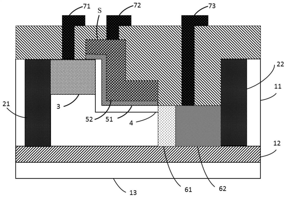
[0032] Embodiment 1, fabricate a tunneling field effect transistor with a length of 3 nm covering the source with the gate.

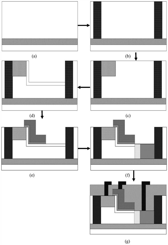
[0033] Step 1, make SOI substrate, such as figure 2 (a).

[0034] 1a) dry oxygen oxidation on the underlying initial silicon wafer to form a buried oxide layer;

[0035] 1b) A top silicon epitaxial layer is grown on the buried oxide layer by an epitaxial growth process to form an SOI substrate.

[0036] Step 2, etching on both sides of the top layer of silicon to form isolation grooves, such as figure 2 (b).

[0037] 2a) First grow SiO on the top silicon surface of SOI substrate 2 Form the first SiO 2 layer, and then grow the first Si on the surface of the layer 3 N 4 layer, forming the first protective layer;

[0038] 2b) using a photolithography machine to form a shallow trench isolation pattern on the first protection layer by a photolithography process;

[0039] 2c) Etching the shallow trench isolation pattern by using a dry etching proce...

Embodiment 2

[0072] Embodiment 2, fabricate a tunneling field effect transistor with a length of 6 nm covering the source with the gate.

[0073] Step 1, making SOI substrate, such as figure 2 (a).

[0074] The specific implementation of this step is the same as Step 1 of Example 1.

[0075] Step 2, etching on both sides of the top layer of silicon to form isolation grooves, such as figure 2 (b).

[0076] The specific implementation of this step is the same as step 2 of embodiment 1.

[0077] Step 3, forming a doping concentration of 10 on the top silicon surface 20 cm -3 source area, such as figure 2 (c).

[0078] The specific implementation of this step is the same as step 3 of embodiment 1.

[0079] Step 4, forming an intrinsic silicon channel region on the top silicon surface, such as figure 2 (d).

[0080] The specific implementation of this step is the same as step 4 of embodiment 1.

[0081] Step five, prepare a Z-shaped gate region, and cover the source with the gate...

Embodiment 3

[0098] Embodiment 3, fabricating a tunneling field effect transistor with a length of 9 nm covering the source with the gate.

[0099] The first step is to make the SOI substrate, such as figure 2 (a).

[0100] The specific implementation of this step is the same as Step 1 of Example 1.

[0101] The second step is to etch and form isolation grooves on both sides of the top silicon, such as figure 2 (b).

[0102] The specific implementation of this step is the same as step 2 of embodiment 1.

[0103] The third step is to form a doping concentration of 10 on the top silicon surface 20 cm -3 source area, such as figure 2 (c).

[0104] The specific implementation of this step is the same as step 3 of embodiment 1.

[0105] The fourth step is to form an intrinsic silicon channel region on the top silicon surface, such as figure 2 (d).

[0106] The specific implementation of this step is the same as step 4 of embodiment 1.

[0107] The fifth step is to prepare the Z-s...


PUM


Abstract

The invention discloses a Z-type heterojunction tunneling field effect transistor having a lightly-doped drain structure and a preparation method thereof, and mainly solves the problems of low on-state current and severe bipolar effect of an existing device. The Z-type heterojunction tunneling field effect transistor comprises an SOI substrate (1), isolation grooves (2), a source region (3), a channel region (4), a drain region (6), a gate region (5) and a conductive layer (7). The isolation grooves (2) are arranged at the two sides of the SOI substrate (1); the source region (3), the channelregion (4) and the drain region (6) are arranged on the upper surface of the SOI substrate; the gate region (5) is arranged on the upper side of the channel region (4); the source region (3) adopts agermanium semiconductor; the gate region (5) adopts a Z-type structure, and gates with the length of 3nm-9nm are covered on the source region; and the side, close to the gate region (5), of the drainregion (6) is provided with a lightly-doped drain region. The Z-type heterojunction tunneling field effect transistor can effectively suppress the bipolar effect and improve driving current, and can be used for manufacturing of a large-scale integrated circuit.

Description

technical field [0001] The invention belongs to the technical field of semiconductor devices, and in particular relates to a Z-type tunneling field effect transistor and a preparation method thereof, which can be used in the manufacture of large-scale integrated circuits. Background technique [0002] With the advancement of semiconductor integration technology, the development of integrated circuit technology following "Moore's law" has entered the nanometer scale. However, challenges from short-channel effects, parasitic effects, and quantum tunneling make it increasingly difficult to scale down conventional CMOS transistors, and it is difficult to meet the requirements of continuous development of integrated circuits. [0003] Tunneling Field Effect Transistor TFET works based on the quantum tunneling effect mechanism of band tunneling. At room temperature, the subthreshold swing can break through the limitation of the traditional MOSFET subthreshold limit value of 60mV / d...

Claims


Application Information

Patent Timeline
Patent Type & Authority Patents(China)
IPC IPC(8): H01L29/739H01L29/165H01L29/423H01L29/08H01L21/331
CPCH01L29/0847H01L29/165H01L29/42356H01L29/66356H01L29/7391
Inventor 李聪闫志蕊庄奕琪赵小龙郭嘉敏
Owner 西安电子科技大学重庆集成电路创新研究院
Why Eureka
Try Eureka